M2204 Master Volume lead 50‑style · 1977–1989 · 50 W

draft
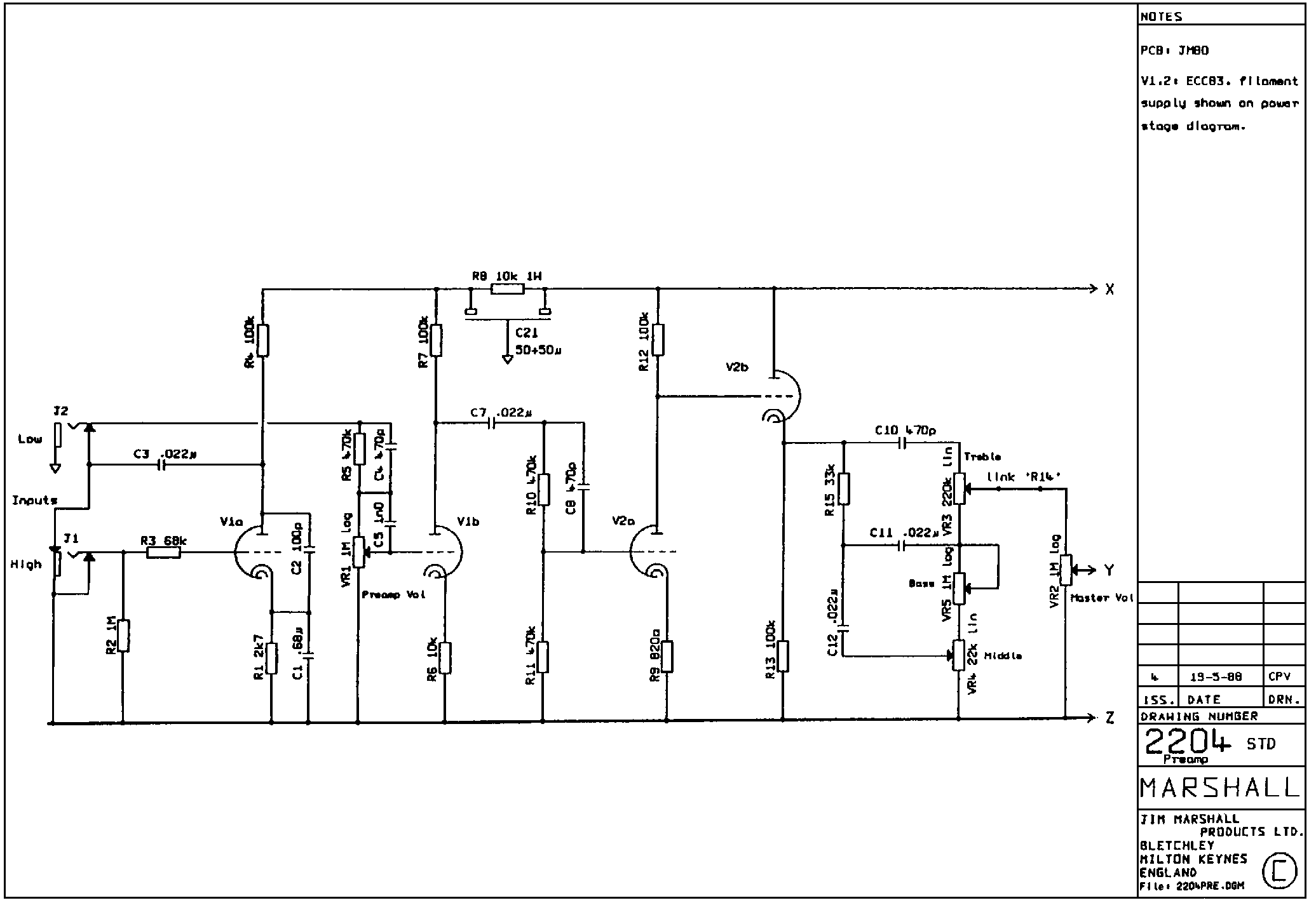
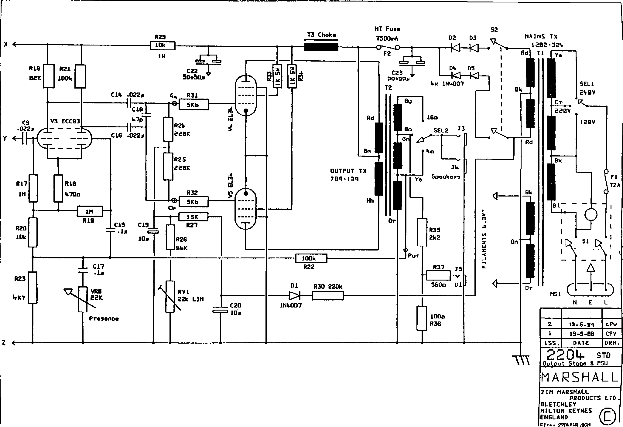
Schematic — redrawn in KiCad · scroll to zoom, drag to pan
Board layout — redrawn reference diagram · source noted on the drawing Print sheet ↗
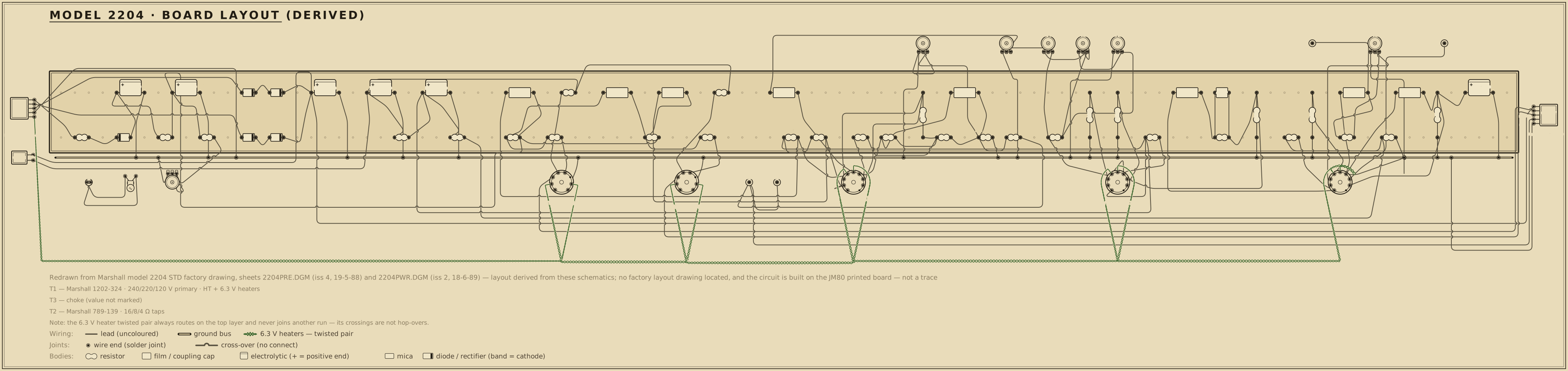
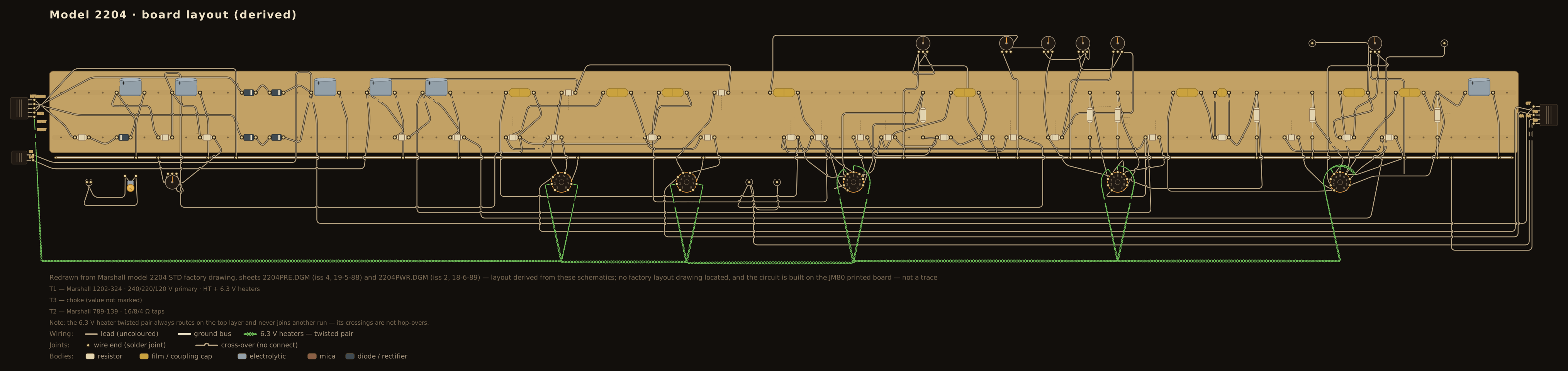
M2204 board layout — an original diagram reconstructed from the redrawn schematic (no factory layout sheet exists), showing the principal parts in board order, drawn in the period layout-sheet style with each value lettered on the part.

Scroll the drawing sideways to read the whole board — the source line and the colour legend run along the bottom of the sheet — or open the full-size diagram in its own tab. Values are lettered on the parts in the period shorthand — .02-400, 250-5, 1MEG: how to read it.

Machine-checked wiring. Every modelled part the operating-point netlist places on this board has been verified in CI, terminal for terminal, to be electrically equivalent to the circuit's simulated netlist. This diagram documents connectivity and part arrangement — it is not a dimensioned 1:1 build template.

Details

The modelled parts are the tube sockets, the plate, cathode and grid-leak resistors, the power-rail droppers, and the coupling and bypass capacitors whose two leads are both named DC nodes; the check proves the same net structure, with no missing or extra connections. Parts outside that DC model — the volume / tone / mixer control-network internals, the negative-bias front end, and the heater chain, pilot lamp and power-transformer / rectifier AC side — are drawn from the cited sources but are not machine-checked; the CI report enumerates every one of their terminals so the boundary is explicit rather than silent.

Board and part positions are drawn at diagram scale, and lead dress, grounding paths, and physical spacing all matter in a high-voltage chassis. If you build from it, verify every connection against the schematic above and the operating-point table below as you go.
Simulated operating point

No published voltage chart exists for this circuit — the factory drawing prints component values only. The voltages below are informational results simulated from the redrawn netlist, not read from or checked against any chart. Because there is no measured reference to verify against, this circuit is published as a draft.

Node Simulated Note
BP2 469.6 V EL34 screen supply node, after the filter choke (the OT centre tap is taken ahead of it, at B+1)
BP3 388.0 V preamp rail X — phase-inverter plates, V2a plate load and V2b plate, after the R29 10 kΩ dropper
BP4 375.2 V input-stage rail — V1a and V1b plate loads, after the R8 10 kΩ dropper
P1A 282.8 V V1a plate — input stage, 100 kΩ load, 2.7 kΩ cathode
K1A 2.5 V V1a cathode (2.7 kΩ; 0.68 µF bypass)
P1B 338.9 V V1b plate — cascaded second stage, 100 kΩ load
K1B 3.6 V V1b cathode (10 kΩ, unbypassed) — the cold, gain-shaping stage the 2204 adds over the 1987
P2A 219.1 V V2a plate — third gain stage (100 kΩ load), DC-coupled to the cathode follower
K2A 1.4 V V2a cathode (820 Ω, unbypassed)
KCF 219.7 V V2b cathode follower output (100 kΩ load) feeding the TMB tone stack
PPIA 258.3 V phase-inverter plate, 82 kΩ side (V3a — the driven side, fed from the master volume)
PPIB 248.1 V phase-inverter plate, 100 kΩ side (V3b)
KPI 44.6 V phase-inverter shared cathode over the 470 Ω cathode resistor
JPI 43.2 V phase-inverter tail junction — both 1 MΩ grid leaks return here, above the 10 kΩ tail
NNFB 13.4 V negative-feedback node at the foot of the tail: 4.7 kΩ to ground, 100 kΩ back to the output-transformer secondary, presence leg capacitor-blocked
SG4 469.6 V V4 screen grid, through its 1.5 kΩ screen resistor (the v0 EL34 fit draws no screen current at this bias, so the drop reads as zero — see notes.md)
SG5 469.6 V V5 screen grid, through its 1.5 kΩ screen resistor

Every node here is simulation-only — there is no published chart to check against — so no chart, deviation or tolerance column is shown.

The output stage behind these numbers can be drawn: the load line explorer plots this circuit's EL34 pair at the DC operating point its netlist carries — 470 V on the plates with a −47 V grid bias — and marks where the load line crosses. This circuit is published as a draft, so that operating point is not verified against a published chart: the table and notes above say what each figure rests on.

Parts list

Every designator in this list appears on the schematic above, and every designator on the schematic appears here — the two are checked against each other in both directions, a valve's two halves counting as one bottle (V1A and V1B are both V1). The drawing prints component values with no wattage or voltage rating except where noted (R8 and R29 are marked 1 W), so ratings are not asserted here. Cathode-bypass and coupling capacitor VALUES are open at DC and do not enter the operating-point netlist; they are listed for completeness. Designators C6, C13 and R28 appear nowhere on either 2204 STD sheet — the JM80 board these sheets document is shared with other models, and unused positions are simply absent from this drawing; they are not omitted here by oversight.

RefPartValue / ratingRole
J1 Jack socket ¼ in mono High-sensitivity input
J2 Jack socket ¼ in mono Low-sensitivity input
R2 Carbon film resistor 1 MΩ Input grid leak
R3 Carbon film resistor 68 kΩ Input grid stopper into V1a
R4 Carbon film resistor 100 kΩ V1a plate load
R1 Carbon film resistor 2.7 kΩ V1a cathode bias
C1 Electrolytic capacitor 0.68 µF V1a cathode bypass
C2 Ceramic capacitor 100 pF Across V1a, plate to cathode — high-frequency shunt
C3 Coupling capacitor 0.022 µF V1a plate → preamp-volume network
R5 Carbon film resistor 470 kΩ Series arm ahead of the preamp volume
C4 Ceramic capacitor 470 pF Bright cap across R5
VR1 Logarithmic potentiometer 1 MΩ Preamp volume
C5 Film capacitor 0.001 µF Bright cap across the preamp volume's upper section (drawn '1n0')
R7 Carbon film resistor 100 kΩ V1b plate load
R6 Carbon film resistor 10 kΩ V1b cathode bias — unbypassed
R8 Power resistor 10 kΩ · 1 W Rail dropper, preamp rail → input-stage rail
C21 Electrolytic capacitor 50 µF + 50 µF Preamp-rail and input-stage-rail filter, one section each side of R8
C7 Coupling capacitor 0.022 µF V1b plate → interstage divider
R10 Carbon film resistor 470 kΩ Interstage divider, series arm
C8 Ceramic capacitor 470 pF Bright cap across R10
R11 Carbon film resistor 470 kΩ Interstage divider, shunt arm — also V2a's grid return
R12 Carbon film resistor 100 kΩ V2a plate load
R9 Carbon film resistor 820 Ω V2a cathode bias — unbypassed
R13 Carbon film resistor 100 kΩ V2b cathode-follower load
R15 Carbon film resistor 33 kΩ Tone-stack slope resistor
C10 Ceramic capacitor 470 pF Tone stack — treble
VR3 Linear potentiometer 220 kΩ Treble
C11 Film capacitor 0.022 µF Tone stack — bass
VR5 Logarithmic potentiometer 1 MΩ Bass — wired as a rheostat, wiper strapped to the top
C12 Film capacitor 0.022 µF Tone stack — middle
VR4 Linear potentiometer 22 kΩ Middle
R14 Wire link wire link Panel link from the treble wiper to the master volume, in the R14 position
VR2 Logarithmic potentiometer 1 MΩ Master volume
C9 Coupling capacitor 0.022 µF Master volume → V3a grid
R17 Carbon film resistor 1 MΩ PI grid leak (V3a), returned to the tail junction
R19 Carbon film resistor 1 MΩ PI grid leak (V3b), returned to the tail junction
R18 Carbon film resistor 82 kΩ PI plate load (V3a, the driven side)
R21 Carbon film resistor 100 kΩ PI plate load (V3b)
R16 Carbon film resistor 470 Ω PI shared cathode resistor
R20 Carbon film resistor 10 kΩ PI tail, junction → feedback node
C15 Film capacitor 0.1 µF AC-grounds V3b's grid to the feedback node
R22 Carbon film resistor 100 kΩ Negative feedback, output-transformer secondary → feedback node
R23 Carbon film resistor 4.7 kΩ Feedback node → ground
C17 Film capacitor 0.1 µF Presence cap, feedback node → presence pot
VR6 Potentiometer 22 kΩ Presence
C14 Coupling capacitor 0.022 µF PI (V3a) → V4 grid
C16 Coupling capacitor 0.022 µF PI (V3b) → V5 grid
C18 Ceramic capacitor 47 pF Phase compensation, across the two output grids
R24 Carbon film resistor 220 kΩ V4 grid leak, from the bias node
R25 Carbon film resistor 220 kΩ V5 grid leak, from the bias node
R31 Carbon film resistor 5.6 kΩ V4 grid stopper
R32 Carbon film resistor 5.6 kΩ V5 grid stopper
R33 Carbon film resistor 1.5 kΩ V4 screen-grid resistor
R34 Carbon film resistor 1.5 kΩ V5 screen-grid resistor
D1 Rectifier diode 1N4007 Bias-supply rectifier
R30 Carbon film resistor 220 kΩ Bias-supply series resistor
C20 Electrolytic capacitor 10 µF Bias-supply reservoir
R27 Carbon film resistor 15 kΩ Bias-supply series resistor into the bias node
R26 Carbon film resistor 56 kΩ Bias divider, upper leg
RV1 Trim potentiometer 22 kΩ Bias adjust
C19 Electrolytic capacitor 10 µF Bias-node filter
D2 Rectifier diode 1N4007 HT bridge rectifier
D3 Rectifier diode 1N4007 HT bridge rectifier
D4 Rectifier diode 1N4007 HT bridge rectifier
D5 Rectifier diode 1N4007 HT bridge rectifier
C23 Electrolytic capacitor 50 µF + 50 µF HT reservoir
F2 Fuse T500 mA HT fuse
T3 Filter choke choke (value not marked) Reservoir → screen-supply choke
C22 Electrolytic capacitor 50 µF + 50 µF Screen-node filter after the choke — both sections of the can land on that node (unlike C21, whose sections straddle R8)
R29 Power resistor 10 kΩ · 1 W Rail dropper, screen node → preamp rail
S2 Toggle switch SPST Standby
T2 Output transformer Marshall 789-139 · 16/8/4 Ω taps Push-pull EL34 output transformer
SEL2 Rotary switch 3-position Speaker impedance selector
J3 Jack socket ¼ in mono Speaker output
J4 Jack socket ¼ in mono Speaker output
R35 Carbon film resistor 2.2 kΩ DI attenuator, series arm off the secondary
R36 Carbon film resistor 100 Ω DI attenuator, shunt arm
R37 Carbon film resistor 560 Ω DI output series resistor
J5 Jack socket ¼ in mono DI output
T1 Power transformer Marshall 1202-324 · 240/220/120 V primary · HT + 6.3 V heaters Mains/HT transformer
SEL1 Voltage selector 240/220/120 V Mains primary selection
F1 Fuse T2 A Mains fuse (T3 A on 120 V)
S1 Toggle switch DPST Mains switch
MS1 Mains inlet N / E / L Mains connector
V1 Preamp tube ECC83 (12AX7) Input stage + cascaded second stage (V1a/V1b)
V2 Preamp tube ECC83 (12AX7) Third gain stage + cathode follower (V2a/V2b)
V3 Preamp tube ECC83 (12AX7) Long-tailed-pair phase inverter (V3a/V3b)
V4 Power tube EL34 Push-pull output (upper)
V5 Power tube EL34 Push-pull output (lower)

Circuit story

The 2204 is the 50-watt lead head after Marshall stopped treating volume as something the player set on the guitar. Two changes do it. The second channel's volume control is repurposed as a master volume between the preamp and the output stage, so the front end can be driven hard at any listening level. And the two input triodes that used to sit side by side as separate channels are wired in series — V1a into a volume control into V1b — so the preamp has three gain stages ahead of the tone stack instead of two.

That cascaded front end is the circuit's whole character. Later it was repackaged, in 1981, with a new cabinet and a new panel and sold as the JCM800.

Circuit walkthrough (short form)

One channel with two inputs. The High jack (J1) runs through a 68 kΩ stopper (R3) with a 1 MΩ leak (R2) into V1a ECC83 (100 kΩ plate, 2.7 kΩ cathode bypassed by 0.68 µF, and a 100 pF cap straight across the triode). V1a's plate couples out through 0.022 µF (C3) into the preamp-volume network — a 470 kΩ series arm (R5) bridged by a 470 pF bright cap (C4) into the 1 MΩ log Preamp Volume (VR1), which carries its own 1 nF cap (C5) across the upper section — and the wiper drives V1b, the cascaded second stage: 100 kΩ plate, and a cold, deliberately unbypassed 10 kΩ cathode. The Low jack (J2) lands on that volume network's own input node rather than on V1a's grid: the drawing wires V1a's coupler to the Low jack's normalling contact, so with nothing plugged into Low the two are joined and the cascaded front end runs normally, and a plug in Low feeds the preamp volume directly — a low-sensitivity input that starts at the second stage.

V1b's plate goes through 0.022 µF (C7) into a 470 kΩ / 470 kΩ divider (R10/R11, with 470 pF across the series arm) — the gain has to be thrown away again before the next stage — into V2a (100 kΩ plate, unbypassed 820 Ω cathode) → V2b cathode follower, DC-coupled (100 kΩ load) → treble-middle-bass tone stack (33 kΩ slope; 470 pF, 0.022 µF and 0.022 µF; 220 kΩ / 1 MΩ / 22 kΩ) → Master Volume (VR2, 1 MΩ log) → 0.022 µF → long-tailed-pair phase inverter (V3: 82 kΩ on the driven plate and 100 kΩ on the other, 470 Ω shared cathode, both 1 MΩ grid leaks to the tail junction, 10 kΩ tail) → 0.022 µF couplers with 47 pF across the grids → EL34 pair, fixed-biased through 220 kΩ grid leaks with 5.6 kΩ grid stoppers and 1.5 kΩ screen resistors → output transformer with 16/8/4 Ω taps. Negative feedback returns from the secondary through 100 kΩ to the foot of the tail, where a 4.7 kΩ resistor to ground and a 22 kΩ presence pot behind a 0.1 µF cap set how much of it comes back at the top end.

Power: a mains transformer with 240/220/120 V primary taps, a four-diode silicon bridge into a 50+50 µF reservoir, an HT fuse and a filter choke. The output transformer's centre tap is taken ahead of the choke, so only the screens and the preamp are fed through it; 10 kΩ / 1 W droppers then step the rail down for the phase inverter and second stage, and again for the input stage. The negative grid bias comes from its own diode, a 220 kΩ series resistor, a 56 kΩ / 22 kΩ adjustable divider and 10 µF filters.

Lineage

The 2204 is the 1987 rewired. Everything from the third gain stage onward — the DC-coupled cathode follower, the tone stack, the long-tailed-pair inverter, the EL34 pair, the presence and feedback network — carries straight across from the 50-watt Plexi, and through it from the JTM45 and the tweed 5F6-A Bassman before that. What changed is in front of it: where the 1987 runs two input triodes as two channels and mixes them through 470 kΩ resistors, the 2204 runs them in series with a volume control between, and puts a second volume control after the tone stack. The output stage also picks up screen resistors and grid stoppers that the 1987 does not have.

The tone network, as the drawing wires it

The 2204 STD sheet wires the stack as the Marshall drawings before it did: the 470 pF treble cap and the 33 kΩ slope resistor both leave the cathode-follower output; one 0.022 µF runs from the slope foot to the node shared by the treble pot's lower lug and the bass pot; the bass pot is a rheostat, its wiper strapped back to its top; the other 0.022 µF feeds the middle pot's wiper; and the stack's output is the treble pot's wiper alone, taken to the master volume through the panel link the drawing labels 'R14'.

A note on verification

Both sheets of the 2204 STD factory drawing print component values only; neither carries a valve-voltage chart. The DC operating points shown for this circuit are simulated from the redrawn netlist rather than compared against a published chart, and the output-stage operating point in particular is an estimate: the corpus's CC0 EL34 model is fitted to a single 250 V datasheet anchor, and this circuit runs its plates near 470 V. Two artefacts of that extrapolation are visible in the figures — a colder-than-real modelling bias is needed to land a physical idle current, and the model's screen current falls to zero at that bias, so the drawn 1.5 kΩ screen resistors show no drop where a real amp would show a few volts. The circuit is therefore published as a draft: its topology and part values are read directly from the factory drawing, but its voltages are not confirmed against a measured reference.

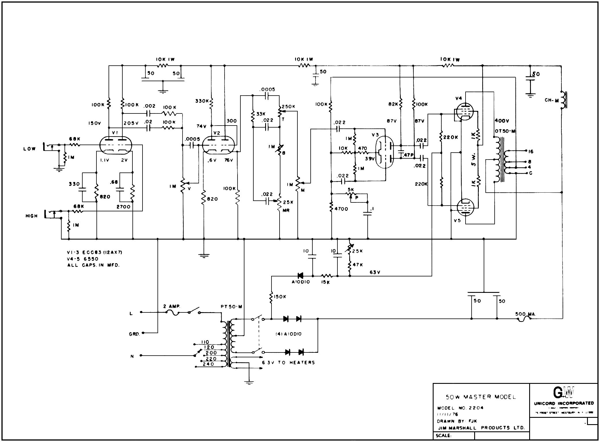
An earlier Marshall drawing of the same model number does print voltages — a '50W MASTER MODEL / MODEL NO. 2204' sheet dated 11/11/76 — but it draws a different circuit: the input triodes still sit in parallel as two channels, and the output valves are a 6550 pair for the US market. That revision predates the series-connected front end this entry documents, so its figures are cited as history, not used as a chart.

Which valves

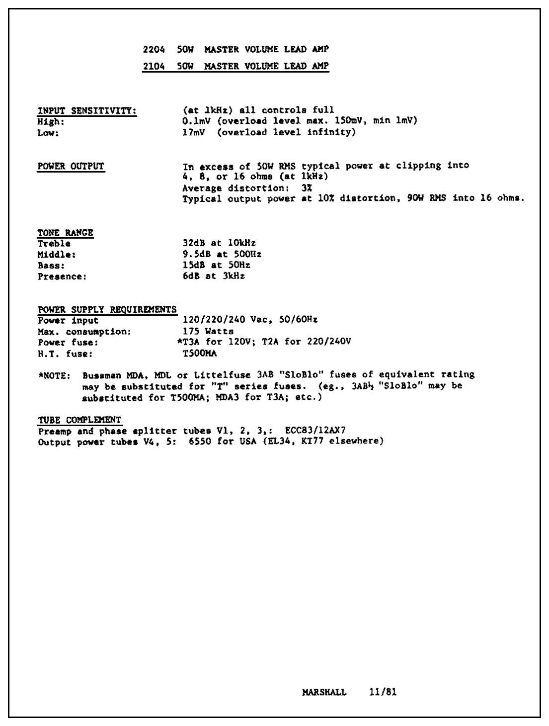
Marshall's own 11/81 specification sheet for the 2204 lists the output pair as "6550 for USA (EL34, KT77 elsewhere)". The EL34 complement documented here is the non-US fitment, and it is the one the 2204 STD drawing itself labels at V4 and V5.

Sources