5F6 Tweed Bassman‑style · 1957–1958 · 40 W

✓ verified 2026-08-02
Schematic — redrawn in KiCad · scroll to zoom, drag to pan
Board layout — redrawn reference diagram · source noted on the drawing Print sheet ↗
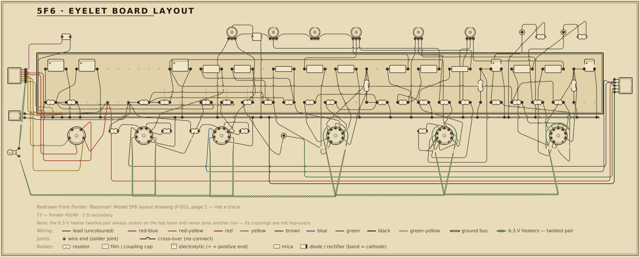
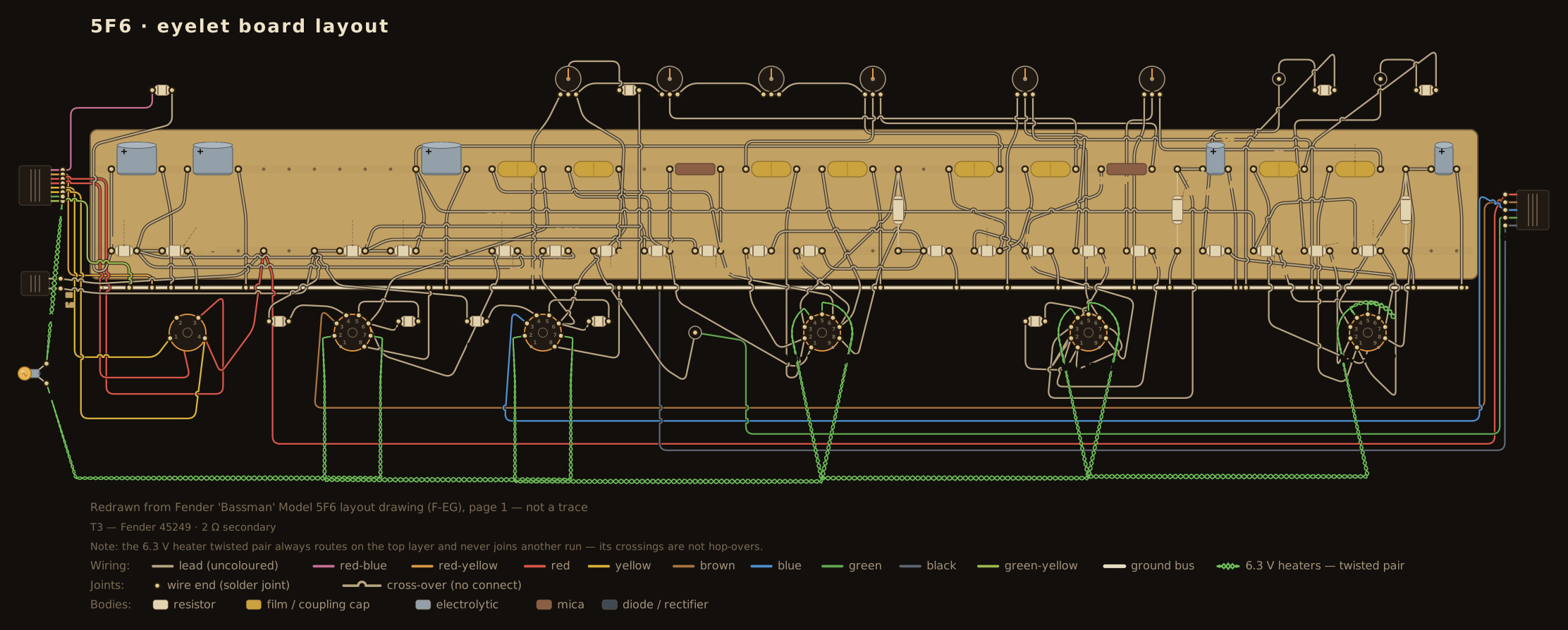
5F6 eyelet board layout — an original diagram redrawn from the published layout drawing, showing the principal parts in the order that drawing places them on the board, drawn in the period layout-sheet style with each value lettered on the part.

Scroll the drawing sideways to read the whole board — the source line and the colour legend run along the bottom of the sheet — or open the full-size diagram in its own tab. Values are lettered on the parts in the period shorthand — .02-400, 250-5, 1MEG: how to read it.

Machine-checked wiring. Every modelled part the operating-point netlist places on this board has been verified in CI, terminal for terminal, to be electrically equivalent to the simulated netlist this circuit is verified against. This diagram documents connectivity and part arrangement — it is not a dimensioned 1:1 build template.

Details

The modelled parts are the tube sockets, the plate, cathode and grid-leak resistors, the power-rail droppers, and the coupling and bypass capacitors whose two leads are both named DC nodes; the check proves the same net structure, with no missing or extra connections. Parts outside that DC model — the volume / tone / mixer control-network internals, the negative-bias front end, and the heater chain, pilot lamp and power-transformer / rectifier AC side — are drawn from the cited sources but are not machine-checked; the CI report enumerates every one of their terminals so the boundary is explicit rather than silent.

Board and part positions are drawn at diagram scale, and lead dress, grounding paths, and physical spacing all matter in a high-voltage chassis. If you build from it, verify every connection against the schematic above and the operating-point table below as you go.

Operating point vs. published chart

Chart values read from the published drawing — or, where the drawing carries no voltage chart, from the cited published measurements (never reproduced). The simulated column is this circuit's own netlist solved in ngspice by the run that gates it; every deviation beside it is those two numbers compared, not a separately stated figure. Tolerances are this project's verification targets: tube-pin nodes carry the tolerance the cited source states, or ±20% — the era's printed convention — where it states none, and power rails are held to tighter internal targets. Every gated node lands within target — worst deviation 9.6%.

Node Chart Simulated Deviation Tolerance Note
BP2 430 V 430.5 V 0.1% ±8% screens node after the choke (DCR estimated at 130 Ω)
BP3 385 V 386.1 V 0.3% ±8% PI supply node after the 4.7 kΩ dropper
BP4 325 V 322.3 V 0.8% ±8% preamp node after the 10 kΩ dropper
PAY1 150 V 164.5 V 9.6% ±20% 12AY7 plate (bright channel), printed pin value
PAY2 150 V 164.5 V 9.6% ±20% 12AY7 plate (normal channel)
KAY 2.5 V 2.6 V 3.5% ±20% shared 12AY7 cathode, 820 Ω
P2A 180 V 181.6 V 0.9% ±20% V2A plate = cathode-follower grid (direct-coupled)
K2A 1.2 V 1.2 V 3.9% ±20% V2A cathode, 820 Ω with a 25 µF bypass
KCF 180 V 182.0 V 1.1% ±20% cathode-follower output, printed +180
PPIA 235 V 252.4 V 7.4% ±20% PI plate, 82k 5% side
PPIB 230 V 242.0 V 5.2% ±20% PI plate, 100k 5% side
KPI 34 V 32.2 V 5.4% ±20% PI cathodes above the 470 Ω tail resistor
JPI 32.5 V 30.7 V 5.5% ±20% tail junction (grid-leak return), above the 10 kΩ to ground
GPIA
chart disputed
22 V 30.7 V 39.6% not gated
The chart contradicts its own topology.

This grid reaches the tail junction through a 1 MΩ leak and has no other DC path, so with no grid current it must sit at the junction's own printed +32.5 V. The printed 22 V is 68% of that — the fraction a 1 MΩ source reads into a meter of roughly 2 MΩ input resistance (22 = 32.5 × 2.1/3.1), which is a 20,000 Ω/V moving-coil voltmeter on its 100 V range rather than the electronic voltmeter the drawing's notice specifies. Simulation follows the topology.

GPIB
chart disputed
23 V 30.7 V 33.5% not gated
The other half of the same contradiction — see GPIA.

Printed 23 V against the same +32.5 V junction is 71%, the same ≈2 MΩ meter loading on the second 1 MΩ leak.

S51 430.4 V informational — 5881 screen after its 100 Ω resistor
G51 −48 V −48.0 V 0.0% ±8% fixed bias via a 220 kΩ leak and a 1.5 kΩ grid stopper from the −48 V supply

Tube-pin nodes are checked at the tolerance the cited source states, or at the era's ±20% convention where it states none; power-rail nodes are held to tighter internal verification targets. A node marked chart disputed is excluded from that check — its printed value contradicts the rest of the chart, and the note says how; its deviation is shown for the record, not as a result. Simulated figures are the netlist's DC solution, not measurements from a chassis.

The output stage behind these numbers can be drawn: the load line explorer plots this circuit's 5881 pair at the DC operating point its netlist carries — 432 V on the plates with a −48 V grid bias — and marks where the load line crosses.

Parts list

Every designator in this list appears on the schematic above, and every designator on the schematic appears here — the two are checked against each other in both directions, a valve's two halves counting as one bottle (V1A and V1B are both V1). Two parts the drawing carries as annotations rather than numbered symbols are listed here without designators, and stand outside that check. Resistor and potentiometer designators are shared with the 5F6-A, so the two revisions read side by side. The capacitor numbers are not, and cannot be: the 5F6 carries two capacitors the 5F6-A does not — the 25 µF across V2A's cathode resistor (C4) and the 47 pF across the phase-inverter plates (C12) — so from C4 onward the two runs diverge and the same C number names a different part on each page. Read a capacitor by its role, not by its number, when comparing the revisions. The parts list covers one jack per channel (the chassis carries four, each channel's second jack adding another 68 kΩ stopper). Speaker jacks, the a-c line and ground switch, the pilot lamp and the standby-switch bypass capacitor are on the chassis, not the board, and are not listed. The output transformer keeps the 5F6-A's T3 for the same reason, which is why no T1 or T2 appears; the power transformer, like the other off-board parts, is listed without a designator.

RefPartValue / ratingRole
R1s Carbon comp resistor 68 kΩ · ½ W Bright-channel grid stopper
R2s Carbon comp resistor 68 kΩ · ½ W Normal-channel grid stopper
RG1 Carbon comp resistor 1 MΩ · ½ W Bright input grid leak
RG2 Carbon comp resistor 1 MΩ · ½ W Normal input grid leak
RL1 Carbon comp resistor 100 kΩ · ½ W V1A plate load
RL2 Carbon comp resistor 100 kΩ · ½ W V1B plate load
RK1 Carbon comp resistor 820 Ω · ½ W Shared 12AY7 cathode bias
C3 Electrolytic capacitor 250 µF · 6 V Shared 12AY7 cathode bypass
C1 Coupling capacitor 0.02 µF · 400 V V1A → bright volume
C2 Coupling capacitor 0.02 µF · 400 V V1B → normal volume
VR1 Audio-taper potentiometer 1 MΩ Bright volume (100 pF bright cap across it)
VR2 Audio-taper potentiometer 1 MΩ Normal volume
RM1 Carbon comp resistor 270 kΩ · ½ W Bright-channel mixer
RM2 Carbon comp resistor 270 kΩ · ½ W Normal-channel mixer
RL3 Carbon comp resistor 100 kΩ · ½ W V2A plate load
RK2 Carbon comp resistor 820 Ω · ½ W V2A cathode bias
C4 Electrolytic capacitor 25 µF · 25 V V2A cathode bypass
RKCF Carbon comp resistor 100 kΩ · ½ W Cathode-follower load
RSL Carbon comp resistor 56 kΩ · ½ W Tone-stack slope resistor
C5 Mica capacitor 250 pF Tone stack — treble
VR3 Potentiometer 250 kΩ Treble
C6 Film capacitor 0.02 µF · 400 V Tone stack — slope junction to the treble/bass node
C7 Film capacitor 0.02 µF · 400 V Tone stack — slope junction to the middle wiper
VR4 Audio-taper potentiometer 1 MΩ Bass (wired as a variable resistor)
VR5 Linear potentiometer 25 kΩ Middle
VR6 Linear potentiometer 5 kΩ Presence — in series with the tone stack's ground leg
C13 Film capacitor 0.1 µF · 200 V Presence wiper to ground
RNF Carbon comp resistor 27 kΩ · ½ W Negative feedback, speaker output → tone-stack ground leg
C10 Coupling capacitor 0.02 µF · 400 V Treble wiper → phase-inverter grid
RGA Carbon comp resistor 1 MΩ · ½ W PI grid leak (V3A), returned to the tail junction
RGB Carbon comp resistor 1 MΩ · ½ W PI grid leak (V3B), returned to the tail junction
RLA Carbon comp resistor 82 kΩ · ½ W · 5% PI plate load (V3A)
RLB Carbon comp resistor 100 kΩ · ½ W · 5% PI plate load (V3B)
RTAIL Carbon comp resistor 470 Ω · ½ W PI tail bias
RT2 Carbon comp resistor 10 kΩ · ½ W PI tail (junction → ground)
C11 Film capacitor 0.1 µF · 200 V V3B grid AC-ground
C12 Mica capacitor 47 pF Across the two PI plates
C8 Coupling capacitor 0.1 µF · 400 V PI → V4 grid
C9 Coupling capacitor 0.1 µF · 400 V PI → V5 grid
RGL1 Carbon comp resistor 220 kΩ · ½ W V4 grid leak, from the −48 V bias line
RGL2 Carbon comp resistor 220 kΩ · ½ W V5 grid leak, from the −48 V bias line
RGS1 Carbon comp resistor 1.5 kΩ · ½ W V4 grid stopper
RGS2 Carbon comp resistor 1.5 kΩ · ½ W V5 grid stopper
RS1 Carbon comp resistor 100 Ω · ½ W V4 screen resistor
RS2 Carbon comp resistor 100 Ω · ½ W V5 screen resistor
RD1 Carbon comp resistor 4.7 kΩ · 1 W Rail dropper B+2 → B+3 (printed 1 W)
RD2 Carbon comp resistor 10 kΩ · 1 W Rail dropper B+3 → B+4 (printed 1 W)
L1 Filter choke Fender 14684 B+1 → B+2 (screens)
C14 Electrolytic capacitor 20 µF · 600 V Filter, B+1
C15 Electrolytic capacitor 20 µF · 600 V Filter, B+1 (second, in parallel with C14)
C16 Electrolytic capacitor 20 µF · 600 V Filter, B+2
C17 Electrolytic capacitor 20 µF · 600 V Filter, B+3
C18 Electrolytic capacitor 8 µF · 450 V Filter, B+4
D1 Rectifier (bias) selenium · silicon diode in modern builds Bias supply rectifier
RB1 Carbon comp resistor 15 kΩ · ½ W Bias supply series resistor
RB2 Carbon comp resistor 56 kΩ · ½ W Bias supply bleeder
C19 Electrolytic capacitor 8 µF · 150 V Bias supply reservoir, rectifier side of the 15 kΩ
C20 Electrolytic capacitor 8 µF · 150 V Bias supply filter, −48 V line
V1 Preamp tube 12AY7 Both input stages (V1A/V1B)
V2 Preamp tube 12AX7 Second stage + cathode follower (V2A/V2B)
V3 Preamp tube 12AX7 Long-tailed-pair phase inverter (V3A/V3B)
V4 Power tube 5881 Push-pull output (upper)
V5 Power tube 5881 Push-pull output (lower)
V6 Rectifier tube 83 Full-wave mercury-vapour rectifier (V6A/V6B)
T3 Output transformer Fender 45249 · 2 Ω secondary Push-pull output into four 8 Ω speakers
Power transformer Fender 8087 · 325-0-325 V HT + heaters + rectifier filament
Mica capacitor 100 pF Bright cap across VR1

Circuit story

The circuit that made the tweed Bassman famous, and the one revision short of the amp everybody copied. Introduced in July 1957, the 5F6 brought in the three-knob treble/middle/bass tone stack, the direct-coupled cathode follower that drives it, the long-tailed-pair phase inverter and the fixed-bias 5881 pair — the whole architecture of the 5F6-A, arriving a year early behind a mercury-vapour rectifier. Produced 1957–1958.

Circuit walkthrough (short form)

Bright + normal channels (1M leaks, 68k stoppers) → V1 12AY7 (100k plates, shared 820 Ω cathode with 250 µF bypass) → 0.02 µF couplers → 1M volume pots (100 pF bright cap) → 270k mixers → V2A 12AX7 (100k plate, 820 Ω cathode with 25 µF bypass) → V2B cathode follower, DC-coupled (100k cathode load) → TMB tone stack (56k slope, 250 pF treble, two 0.02 µF caps; 250k/1M/25k pots) → 0.02 µF → long-tailed-pair PI: 82k (5%) and 100k (5%) plates, 470 Ω + 10k tail, both 1M grid leaks returned to the tail junction, 47 pF across the plates → 0.1 µF couplers → 5881 pair, fixed-biased at −48 V through 220k leaks and 1.5 kΩ grid stoppers, 100 Ω screen resistors → output transformer into four speakers, with 27k of negative feedback returning into the tone stack's ground leg.

Power: 325-0-325 (PT 8087) → 83 → standby → +432 V plates (two 20 µF) → choke (14684) → +430 V screens → 4.7 kΩ → +385 V PI (20 µF) → 10k → +325 V preamp (8 µF). Bias supply: selenium rectifier, 15k/56k, two 8 µF/150 V → −48 V.

The tone network, as the drawings wire it

The published 5F6 schematic and its factory layout sheet agree on a tone-stack wiring that differs from the textbook redrawing of these same parts, and the schematic and layout here follow the sheets:

  • The 250 pF treble capacitor and the 56 kΩ slope resistor both leave the cathode-follower output.
  • One 0.02 µF capacitor runs from the slope resistor's foot to the node shared by the treble pot's lower lug and the bass pot — the treble pot's cold end sits on the far side of that capacitor, not on the slope foot.
  • The bass pot is a rheostat: the layout sheet straps its wiper, and the pot stands in series between that node and the middle pot's top lug.
  • The other 0.02 µF runs from the slope foot to the middle pot's wiper, so the Middle control slides the capacitor's injection point along a 25 kΩ leg that never leaves the circuit.
  • The stack's output is the treble pot's wiper alone; the middle pot's foot returns to ground through the 5 kΩ presence pot.

The textbook form of this stack ties the treble pot's cold end to the slope foot, joins the treble and bass wipers at one output node, and hangs the mid capacitor on top of a rheostat-wired middle pot. The two networks share every part value and differ audibly at the stops: as drawn, the fixed 25 kΩ leg keeps the stack from ever going fully silent with Bass and Middle at zero, where the textbook network's output falls to ground. The tone-stack lab plots this circuit with the wiring the sheets draw.

The 83, and what a mercury-vapour rectifier does to a supply

The 83 is the only mercury-vapour tube in the corpus, and it behaves nothing like the vacuum rectifiers around it. A 5Y3 or a 5U4 is a space-charge device: its forward drop climbs steeply with current, so the B+ falls away on loud notes — the sag that tweed amps are loved for. The 83 instead strikes an arc in mercury vapour, and once struck the drop is pinned near 15 V and stays there from idle to the tube's full 225 mA. Its datasheet says as much in one line: the tube supplies d-c current at essentially constant voltage in spite of rather wide variations in output current.

The practical result is a stiff supply. It is also a demanding one, and the datasheets say so in their ratings rather than in prose. The tube is specified for vertical, base-down mounting. Its condensed mercury has to sit between 20 °C and 60 °C. And the supply must present at least 50 Ω per plate — more if the first filter capacitor exceeds 40 µF — to keep the peak charging current inside the 1 A per-plate limit. The chassis carries a standby switch ahead of the first filter capacitor, which lets the filament come up before the high voltage does. Every one of those conditions goes away with the 5F6-A's indirectly-heated GZ34.

What changed on the way to the 5F6-A

Both drawings print the same rails (+432/+430/+385/+325), the same −48 V bias, the same transformer set (8087 power, 14684 choke, 45249 output) and the same preamp values, so the differences are narrow and specific:

  • Rectifier. The 83 gives way to the GZ34.
  • Presence. On the 5F6 the 5 kΩ presence control sits in the tone stack's ground leg, below the middle pot, with the 27k feedback resistor landing on that same junction and a 0.1 µF cap from the presence wiper to ground; the phase-inverter tail's 10k returns straight to ground. The 5F6-A moves the presence pot, its cap and the feedback return down to the phase-inverter tail, and runs the middle pot's foot straight to ground instead.
  • Output stage. The 5F6's 1.5 kΩ grid stoppers and 100 Ω screen resistors become no stoppers and 470 Ω 1 W screen resistors.
  • Second-stage cathode. The 5F6 bypasses V2A's 820 Ω cathode resistor with 25 µF; the 5F6-A leaves the same resistor unbypassed. It costs the later amp gain at the bottom of the band before the tone stack ever sees the signal.
  • Output transformer secondary. Both sheets print the same 45249 and the same 2 Ω secondary for four 8 Ω speakers.

One thing to watch when reading the two parts lists together: the resistor and pot designators are shared, but the capacitor numbers are not. This amp carries two capacitors the 5F6-A does not — the 25 µF on V2A's cathode and the 47 pF across the phase-inverter plates — so the C run diverges from C4 onward and the same number names a different part on each page. Compare capacitors by role.

Verification — against the printed factory chart

The F-EG drawing prints a full voltage chart, and simulation matches all fourteen gated nodes: rails within 0.8 %, every tube pin within 9.6 % against the chart's own ±20 % convention. Two printed values are excluded, and the reason is arithmetic rather than judgement. The chart gives both phase-inverter grids (+22 V and +23 V) alongside the tail junction they return to (+32.5 V) — but each grid reaches that junction through a 1 MΩ leak and nothing else, so with no grid current both must sit at the junction's own potential. The printed figures are 68 % and 71 % of it, the fraction a 1 MΩ source reads into a meter of roughly 2 MΩ input resistance. They are the signature of a moving-coil voltmeter loading the node, not of a circuit that behaves that way.

The one place the drawing invites a second look is the phase-inverter tail. It is 10k with a 470 Ω bias resistor, and the chart's own +32.5 V junction figure confirms it: 32.5 V across 10k is 3.25 mA, and the printed plate drops (385→235 V through 82k, 385→230 V through 100k) imply about 3.4 mA through the pair — the same current, inside the chart's own precision.

Sources