M1987 Plexi lead 50-style · 1967–1981 · 50 W

draft
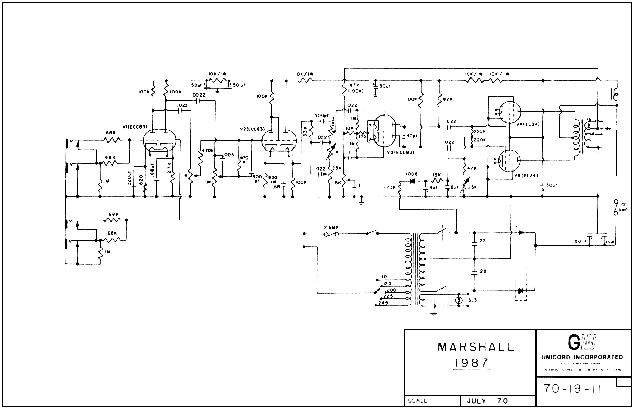
Schematic — redrawn in KiCad · scroll to zoom, drag to pan
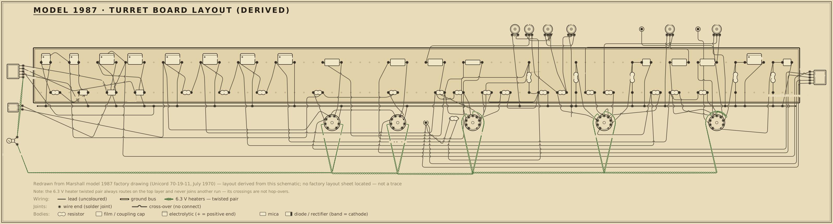
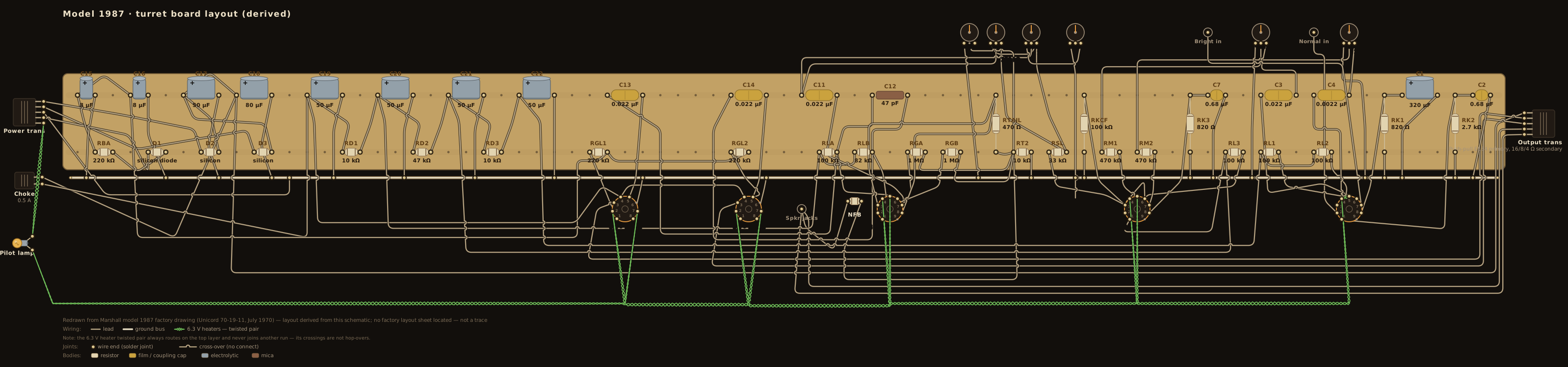
Board layout — redrawn reference diagram · source noted on the drawing
M1987 turret board layout — an original diagram reconstructed from the redrawn schematic (no factory layout sheet exists), showing the principal parts in board order.

Machine-checked wiring. Every modelled part the operating-point netlist places on this board — the tube sockets, the plate, cathode and grid-leak resistors, the power-rail droppers, and the coupling and bypass capacitors whose two leads are both named DC nodes — has been verified in CI, terminal for terminal, to be electrically equivalent to the circuit's simulated netlist: the same net structure, no missing or extra connections. Parts outside that DC model — the volume / tone / mixer control-network internals, the negative-bias front end, and the heater chain, pilot lamp and power-transformer / rectifier AC side — are drawn from the cited sources but are not machine-checked; the CI report enumerates every one of their terminals so the boundary is explicit rather than silent. This diagram documents connectivity and part arrangement — it is not a dimensioned 1:1 build template. Board and part positions are drawn at diagram scale, and lead dress, grounding paths, and physical spacing all matter in a high-voltage chassis. If you build from it, verify every connection against the schematic above and the operating-point table below as you go.
Simulated operating point

No published voltage chart exists for this circuit — the factory drawing prints component values only. The voltages below are informational results simulated from the redrawn netlist, not read from or checked against any chart. Because there is no measured reference to verify against, this circuit is published as a draft.

NodeChartToleranceNote
BP2 EL34 screen-grid supply node, after the filter choke (~B+1)
BP3 phase-inverter supply node
BP4 second-stage / cathode-follower supply node, after the 47 kΩ dropper
BP5 input-stage supply node, after the 10 kΩ dropper
P1A V1A plate — channel I (high-treble) input, 100 kΩ load, 820 Ω cathode
K1A V1A cathode (820 Ω; 320 µF bypass)
P1B V1B plate — channel II (normal) input, 100 kΩ load, 2.7 kΩ cathode
K1B V1B cathode (2.7 kΩ; 0.68 µF bypass) — the colder-biased channel
P2A V2A plate — second gain stage (100 kΩ load), DC-coupled to the cathode follower
K2A V2A cathode (820 Ω; 0.68 µF bypass)
KCF V2B cathode follower output (100 kΩ load) feeding the TMB tone stack
PPIA phase-inverter plate, 100 kΩ side (V3A)
PPIB phase-inverter plate, 82 kΩ side (V3B)
KPI phase-inverter shared cathode over the 470 Ω / 10 kΩ tail

Every node here is simulation-only — there is no published chart to check against — so no chart column or tolerance is shown.

Parts list

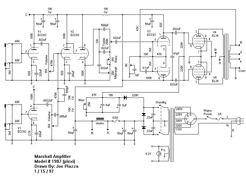
Reference designators match the schematic above. Cathode-bypass and coupling capacitor VALUES are open at DC and do not enter the operating-point netlist; they are listed for completeness. The Joe Piazza redraw prints the V1B/V2A bypass caps as 68 µF where this factory drawing reads 0.68 µF — the factory value is used (see meta.yaml).

RefPartValue / ratingRole
R1s Carbon comp resistor 68 kΩ · ½ W Channel I high-treble input grid stopper
R2s Carbon comp resistor 68 kΩ · ½ W Channel I normal input grid stopper
R3s Carbon comp resistor 68 kΩ · ½ W Channel II high input grid stopper
R4s Carbon comp resistor 68 kΩ · ½ W Channel II low input grid stopper
RG1 Carbon comp resistor 1 MΩ · ½ W Channel I input grid leak
RG2 Carbon comp resistor 1 MΩ · ½ W Channel II input grid leak
RL1 Carbon comp resistor 100 kΩ · ½ W V1A plate load (channel I)
RL2 Carbon comp resistor 100 kΩ · ½ W V1B plate load (channel II)
RK1 Carbon comp resistor 820 Ω · ½ W V1A cathode bias (channel I)
C1 Electrolytic capacitor 320 µF · 6 V V1A cathode bypass
RK2 Carbon comp resistor 2.7 kΩ · ½ W V1B cathode bias (channel II — the colder channel)
C2 Film capacitor 0.68 µF V1B cathode bypass (partial)
C3 Coupling capacitor 0.022 µF · 400 V V1A → channel I volume
C4 Coupling capacitor 0.0022 µF · 400 V V1B → channel II volume
VR1 Audio-taper potentiometer 1 MΩ Channel I (high-treble) volume
VR2 Audio-taper potentiometer 1 MΩ Channel II (normal) volume
C5 Film capacitor 0.005 µF Channel I bright/treble-bleed cap
C6 Mica capacitor 500 pF Channel II bright cap
RB1 Carbon comp resistor 470 kΩ · ½ W Channel I bright-network resistor
RB2 Carbon comp resistor 470 kΩ · ½ W Channel II bright-network resistor
RM1 Carbon comp resistor 470 kΩ · ½ W Channel I mixing resistor into V2A grid
RM2 Carbon comp resistor 470 kΩ · ½ W Channel II mixing resistor into V2A grid
RL3 Carbon comp resistor 100 kΩ · ½ W V2A plate load (second stage)
RK3 Carbon comp resistor 820 Ω · ½ W V2A cathode bias (drawing annotates a 1 kΩ variant)
C7 Film capacitor 0.68 µF V2A cathode bypass (partial)
RKCF Carbon comp resistor 100 kΩ · ½ W V2B cathode-follower load
RSL Carbon comp resistor 33 kΩ · ½ W Tone-stack slope resistor
C8 Mica capacitor 500 pF Tone stack — treble
VR3 Potentiometer 250 kΩ Treble
C9 Film capacitor 0.022 µF · 400 V Tone stack — bass
VR4 Audio-taper potentiometer 1 MΩ Bass
C10 Film capacitor 0.022 µF · 400 V Tone stack — middle
VR5 Linear potentiometer 25 kΩ Middle
C11 Coupling capacitor 0.022 µF · 400 V Tone stack → phase-inverter grid
RGA Carbon comp resistor 1 MΩ · ½ W PI grid leak (V3A), returned to the tail junction
RGB Carbon comp resistor 1 MΩ · ½ W PI grid leak (V3B), returned to the tail junction
RLA Carbon comp resistor 100 kΩ · ½ W PI plate load (V3A)
RLB Carbon comp resistor 82 kΩ · ½ W PI plate load (V3B)
RTAIL Carbon comp resistor 470 Ω · ½ W PI tail (shared cathode → junction)
RT2 Carbon comp resistor 10 kΩ · ½ W PI tail (junction → NFB/ground)
C12 Mica capacitor 47 pF PI plate-to-plate / phase compensation
C13 Coupling capacitor 0.022 µF · 400 V PI → V4 grid
C14 Coupling capacitor 0.022 µF · 400 V PI → V5 grid
RGL1 Carbon comp resistor 220 kΩ · ½ W V4 grid leak, from the bias line
RGL2 Carbon comp resistor 220 kΩ · ½ W V5 grid leak, from the bias line
D1 Rectifier (bias) silicon diode Bias-supply rectifier
RBA Carbon comp resistor 220 kΩ · ½ W Bias-supply divider/series resistor
RBB Carbon comp resistor 15 kΩ · ½ W Bias-supply series resistor
VR6 Trim potentiometer 25 kΩ Bias adjust
RBC Carbon comp resistor 47 kΩ · ½ W Bias-supply resistor
C15 Electrolytic capacitor 8 µF Bias-supply filter
C16 Electrolytic capacitor 8 µF Bias-supply filter
RD1 Power resistor 10 kΩ · 1 W Rail dropper B+2 (screens) → B+3 (phase inverter)
RD2 Power resistor 47 kΩ · 1 W Rail dropper B+3 (phase inverter) → B+4 (second stage / cathode follower) — drawing annotates a 100 kΩ variant
RD3 Power resistor 10 kΩ · 1 W Rail dropper B+4 (second stage) → B+5 (input stage)
L1 Filter choke 0.5 A Reservoir → screen-supply choke
C17 Electrolytic capacitor 50 µF · 500 V Reservoir filter (B+1)
C18 Electrolytic capacitor 80 µF · 500 V Reservoir filter (B+1)
C19 Electrolytic capacitor 50 µF · 500 V Screen-node filter
C20 Electrolytic capacitor 50 µF · 500 V Phase-inverter-supply filter
C21 Electrolytic capacitor 50 µF · 350 V Second-stage-supply filter
C22 Electrolytic capacitor 50 µF · 350 V Input-stage-supply filter
D2 Rectifier diode silicon HT full-wave rectifier (upper)
D3 Rectifier diode silicon HT full-wave rectifier (lower)
C23 Film capacitor 0.022 µF Rectifier diode snubber
C24 Film capacitor 0.022 µF Rectifier diode snubber
V1 Preamp tube ECC83 (12AX7) Input valve — both channels (V1A/V1B)
V2 Preamp tube ECC83 (12AX7) Second stage + cathode follower (V2A/V2B)
V3 Preamp tube ECC83 (12AX7) Long-tailed-pair phase inverter (V3A/V3B)
V4 Power tube EL34 Push-pull output (upper)
V5 Power tube EL34 Push-pull output (lower)
T1 Output transformer Push-pull EL34 primary, 16/8/4 Ω secondary Output transformer
Power transformer Universal primary 110/120/200/225/245 V · HT + 6.3 V heaters Mains/HT transformer
Fuse 2 A Mains fuse (annotation)
Fuse ½ A HT fuse (annotation)
Standby switch SPST HT standby (annotation)
Pilot lamp 6.3 V Panel pilot lamp (annotation)
Carbon comp resistor presence/NFB network Negative-feedback + presence around the PI tail (annotation)

Circuit story

The Marshall model 1987 is the 50-watt lead head at the centre of the "Plexi" sound. It is the JTM45 grown up: the same four-input, two-channel front end and cathode-follower tone stack, but with a pair of EL34 pentodes in place of the JTM45's KT66 beam tetrodes and a solid-state rectifier in place of the GZ34. Those two changes — a higher, stiffer rail behind faster output valves — are much of what turned the JTM45's bluesy roar into the brighter, harder-edged voice of late-1960s British rock.

"Plexi" names the circuit and its voicing, not the panel: Marshall switched from the gold acrylic (Perspex) front panel to a brushed-metal panel around 1969, so the factory drawing cited here (Unicord, July 1970) is metal-panel era.

Circuit walkthrough (short form)

Two channels, each with high and low inputs (68 kΩ stoppers, 1 MΩ leaks) → V1 ECC83, one triode per channel (100 kΩ plates). The two channels are deliberately unmatched: the high-treble channel runs an 820 Ω cathode fully bypassed by 320 µF, while the normal channel runs a colder 2.7 kΩ cathode with a 0.68 µF partial bypass. Each plate feeds its own 1 MΩ volume control (with a bright cap) and the channels mix through 470 kΩ resistors into V2A (100 kΩ plate, 820 Ω / 0.68 µF cathode) → V2B cathode follower, DC-coupled (100 kΩ load) → treble-middle-bass tone stack (33 kΩ slope; 500 pF, 0.022 µF and 0.022 µF; 250 kΩ / 1 MΩ / 25 kΩ) → long-tailed-pair phase inverter (V3: 100 kΩ and 82 kΩ plates, 470 Ω + 10 kΩ tail, both 1 MΩ grid leaks to the tail junction, 47 pF across) → 0.022 µF couplers → EL34 pair, fixed-biased through 220 kΩ grid leaks → output transformer with 16/8/4 Ω taps, negative feedback and a presence control returned to the tail.

Power: a universal-primary mains transformer (110/120/200/225/245 V taps) and a silicon full-wave rectifier feed a 50 µF + 80 µF reservoir; a filter choke and a chain of 10 kΩ / 1 W droppers (with a 47 kΩ dropper to the phase-inverter/second- stage supply) step the rail down for the screens, phase inverter and preamp. The negative grid bias comes from a diode, a 220 kΩ / 15 kΩ / 25 kΩ network and 8 µF filters.

Lineage

The 1987 descends directly from the JTM45, and through it from the tweed 5F6-A Bassman the JTM45 copied. The signal path is nearly the same stage for stage; the differences are the ones that define the Plexi. The KT66 output pair becomes a pair of EL34 pentodes — more transconductance and a sharper overdrive — and the GZ34 valve rectifier becomes silicon diodes, which hold the rail up harder under load. The input valve stays an ECC83, and the four-input two-channel layout, the DC-coupled cathode follower and the long-tailed-pair inverter all carry straight across.

A note on verification

Marshall drawings of this period print component values only; the model 1987 factory drawing carries no valve-voltage chart. The DC operating points shown for this circuit are simulated from the redrawn netlist rather than compared against a published chart, and the output-stage operating point in particular is an estimate only. The circuit is therefore published as a draft: its topology and part values are read directly from the factory drawing and cross-checked against a second published redraw, but its voltages are not yet confirmed against a measured reference.

Sources