JTM45 British lead-style · 1962–1966 · 45 W

✓ verified 2026-07-18
Schematic — redrawn in KiCad · scroll to zoom, drag to pan
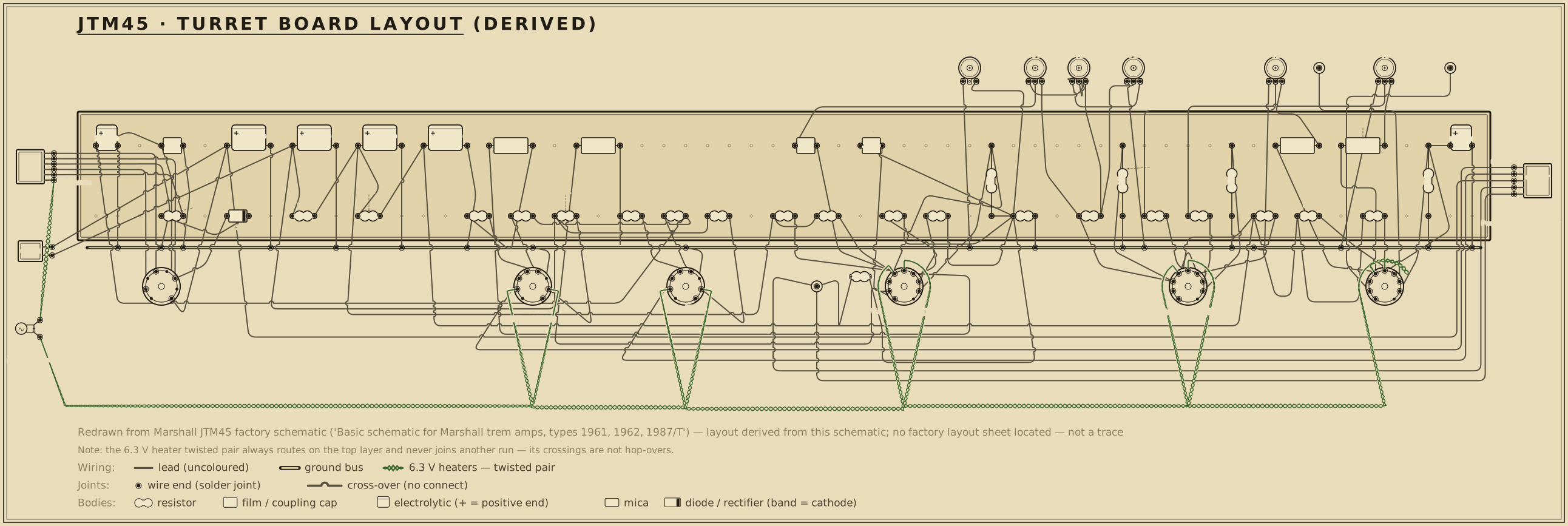
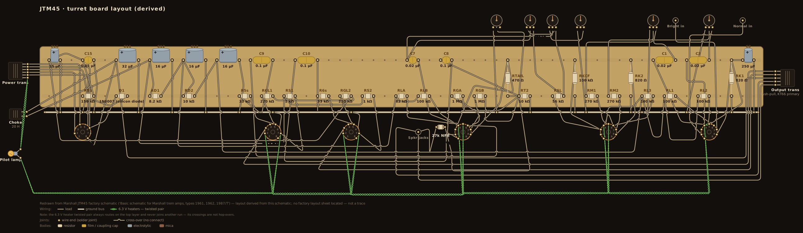
Board layout — redrawn reference diagram · source noted on the drawing
JTM45 turret board layout — an original diagram reconstructed from the redrawn schematic (no factory layout sheet exists), showing the principal parts in board order.

Machine-checked wiring. Every modelled part the operating-point netlist places on this board — the tube sockets, the plate, cathode and grid-leak resistors, the power-rail droppers, and the coupling and bypass capacitors whose two leads are both named DC nodes — has been verified in CI, terminal for terminal, to be electrically equivalent to the simulated netlist this circuit is verified against: the same net structure, no missing or extra connections. Parts outside that DC model — the volume / tone / mixer control-network internals, the negative-bias front end, and the heater chain, pilot lamp and power-transformer / rectifier AC side — are drawn from the cited sources but are not machine-checked; the CI report enumerates every one of their terminals so the boundary is explicit rather than silent. This diagram documents connectivity and part arrangement — it is not a dimensioned 1:1 build template. Board and part positions are drawn at diagram scale, and lead dress, grounding paths, and physical spacing all matter in a high-voltage chassis. If you build from it, verify every connection against the schematic above and the operating-point table below as you go.
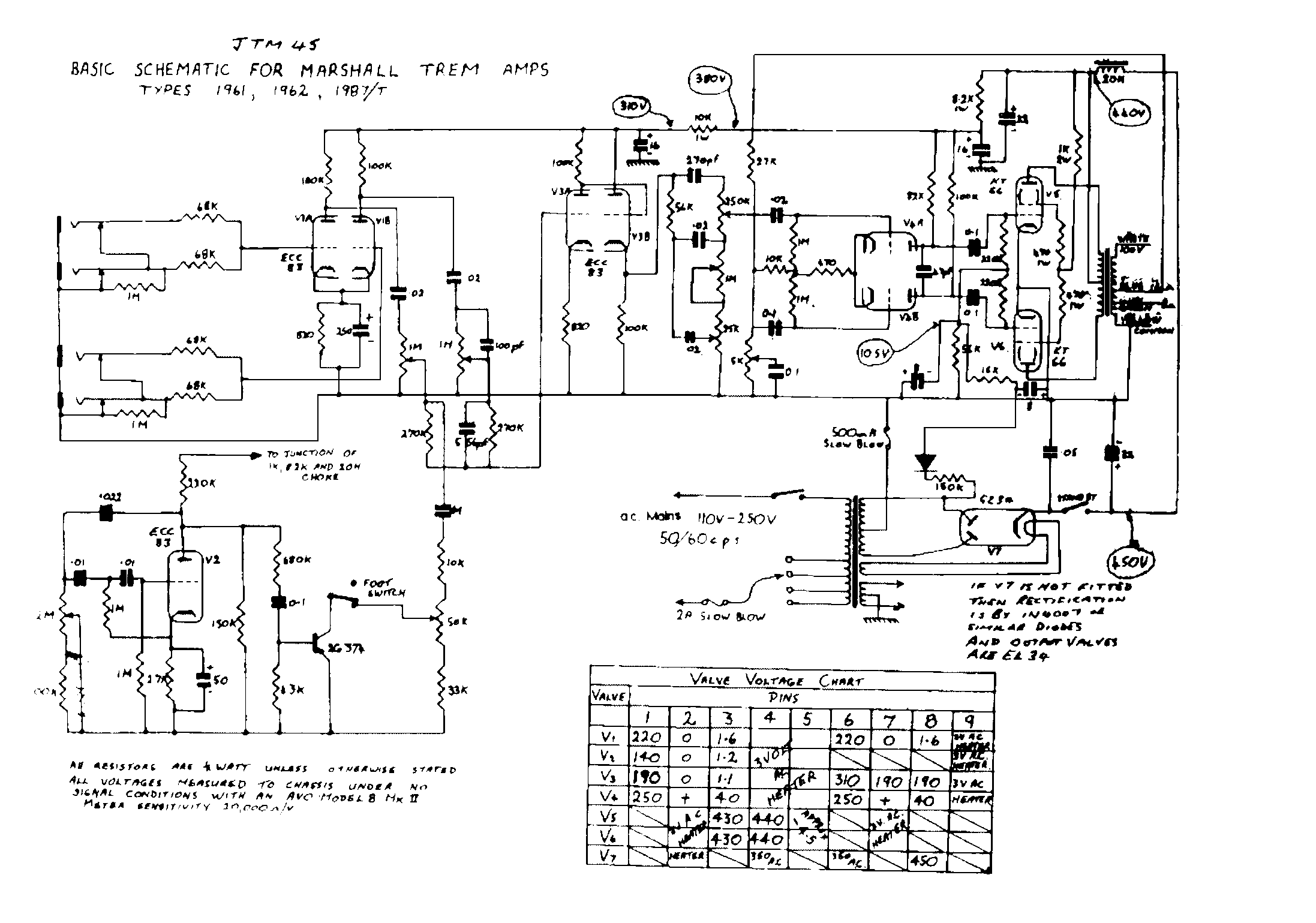
Operating point vs. published chart

Chart values read from the published drawing — or, where the drawing carries no voltage chart, from the cited published measurements (never reproduced). Tolerances are this project's verification targets — tighter on power rails than the ±20% measurement convention Fender printed on its charts. Simulation matches every node within target — worst deviation 9.5%.

NodeChartToleranceNote
BP2 440 V ±8% screens node after the 20H choke (DCR estimated); the anchor-point KT66 model draws little screen current here, so the simulated choke drop is smaller than the chart's
BP3 380 V ±8% PI supply node after the 8.2 kΩ dropper
BP4 310 V ±8% preamp node after the 10 kΩ dropper
P1A 220 V ±20% ECC83 input plate (bright)
P1B 220 V ±20% ECC83 input plate (normal)
KA 1.6 V ±20% shared ECC83 input cathode, 820 Ω
P3A 190 V ±20% V3A plate = cathode-follower grid (direct-coupled)
K3A 1.1 V ±20% V3A cathode, 820 Ω
KCF 190 V ±20% cathode-follower output (chart V3 pin 8)
PPIA 250 V ±20% PI plate, 82 kΩ side
PPIB 250 V ±20% PI plate, 100 kΩ side
KPI 40 V chart disputed The printed 40 V contradicts the chart's own 250 V plate figures: 40 V across the 10 kΩ tail implies ~3.8 mA, which would pull the 82k/100k plates to ~190–225 V. Simulation reproduces the printed plates exactly and settles the cathode near 31 V — the same value the identical phase-inverter stage measures in the 5F6-A.
JPI tail junction; the drawing marks the PI grids only as '+' (qualitative)
S5 informational — KT66 screen after the 1 kΩ stopper (chart screen 440 V ≈ B+2)

Tube-pin nodes are checked against the chart's own printed ±20% convention; power-rail nodes are held to tighter internal verification targets.

Parts list

Reference designators match the schematic above. The schematic draws one jack per channel (the chassis has four). This is the plain (non-tremolo) head: the factory drawing's V2 tremolo valve and its bias-modulation network are omitted, so the valve numbering follows the drawing (V1 input, V3 second stage + cathode follower, V4 phase inverter, V5/V6 KT66, V7 GZ34). Parts drawn only as annotations (bright cap, NFB, presence, presence cap) are listed without designators.

RefPartValue / ratingRole
R1s Carbon comp resistor 68 kΩ · ½ W Bright-channel grid stopper
R2s Carbon comp resistor 68 kΩ · ½ W Normal-channel grid stopper
RG1 Carbon comp resistor 1 MΩ · ½ W Bright input grid leak
RG2 Carbon comp resistor 1 MΩ · ½ W Normal input grid leak
RL1 Carbon comp resistor 100 kΩ · ½ W V1A plate load
RL2 Carbon comp resistor 100 kΩ · ½ W V1B plate load
RK1 Carbon comp resistor 820 Ω · ½ W Shared ECC83 input cathode bias
C3 Electrolytic capacitor 250 µF · 6 V Shared input cathode bypass
C1 Coupling capacitor 0.02 µF · 400 V V1A → bright volume
C2 Coupling capacitor 0.02 µF · 400 V V1B → normal volume
VR1 Audio-taper potentiometer 1 MΩ Bright volume (100 pF bright cap across it)
VR2 Audio-taper potentiometer 1 MΩ Normal volume
RM1 Carbon comp resistor 270 kΩ · ½ W Bright-channel mixer
RM2 Carbon comp resistor 270 kΩ · ½ W Normal-channel mixer
RL3 Carbon comp resistor 100 kΩ · ½ W V3A plate load
RK2 Carbon comp resistor 820 Ω · ½ W V3A cathode bias
RKCF Carbon comp resistor 100 kΩ · ½ W Cathode-follower load
RSL Carbon comp resistor 56 kΩ · ½ W Tone-stack slope resistor
C4 Mica capacitor 270 pF Tone stack — treble
VR3 Potentiometer 250 kΩ Treble
C5 Film capacitor 0.02 µF · 400 V Tone stack — bass
VR4 Audio-taper potentiometer 1 MΩ Bass
C6 Film capacitor 0.01 µF · 400 V Tone stack — middle
VR5 Linear potentiometer 25 kΩ Middle
C7 Coupling capacitor 0.02 µF · 400 V Tone stack → phase-inverter grid
RGA Carbon comp resistor 1 MΩ · ½ W PI grid leak (V4A), returned to tail junction
RGB Carbon comp resistor 1 MΩ · ½ W PI grid leak (V4B), returned to tail junction
RLA Carbon comp resistor 82 kΩ · ½ W PI plate load (V4A)
RLB Carbon comp resistor 100 kΩ · ½ W PI plate load (V4B)
RTAIL Carbon comp resistor 470 Ω · ½ W PI tail bias
RT2 Carbon comp resistor 10 kΩ · ½ W PI tail (junction → foot)
C8 Film capacitor 0.1 µF · 400 V V4B grid AC-ground to the tail junction
C9 Coupling capacitor 0.1 µF · 400 V PI → V5 grid
C10 Coupling capacitor 0.1 µF · 400 V PI → V6 grid
R5s Carbon comp resistor 33 kΩ · ½ W V5 grid stopper
R6s Carbon comp resistor 33 kΩ · ½ W V6 grid stopper
RGL1 Carbon comp resistor 220 kΩ · ½ W V5 grid leak, from the −50 V bias line
RGL2 Carbon comp resistor 220 kΩ · ½ W V6 grid leak, from the −50 V bias line
RS1 Carbon comp resistor 1 kΩ · 2 W V5 screen resistor
RS2 Carbon comp resistor 1 kΩ · 2 W V6 screen resistor
RD1 Power resistor 8.2 kΩ · 1 W Rail dropper B+2 → B+3
RD2 Power resistor 10 kΩ · 1 W Rail dropper B+3 → B+4
L1 Filter choke 20 H B+1 → B+2 (screens)
C11 Electrolytic capacitor 32 µF · 500 V Reservoir filter, B+1
C12 Electrolytic capacitor 16 µF · 500 V Filter, B+2
C13 Electrolytic capacitor 16 µF · 500 V Filter, B+3
C14 Electrolytic capacitor 16 µF · 450 V Filter, B+4
D1 Rectifier (bias) 1N4007 (silicon diode) Bias supply rectifier
RB1 Carbon comp resistor 150 kΩ · ½ W Bias supply series resistor
C15 Film capacitor 0.05 µF · 350 V Bias supply filter
C16 Electrolytic capacitor 25 µF · 50 V Bias supply reservoir
V1 Preamp tube ECC83 (12AX7) Both input stages (V1A/V1B)
V3 Preamp tube ECC83 (12AX7) Second stage + cathode follower (V3A/V3B)
V4 Preamp tube ECC83 (12AX7) Long-tailed-pair phase inverter (V4A/V4B)
V5 Power tube KT66 Push-pull output (upper)
V6 Power tube KT66 Push-pull output (lower)
V7 Rectifier tube GZ34 Full-wave rectifier (V7A/V7B)
T3 Output transformer Push-pull, KT66 primary Push-pull output to the speaker
Power transformer 360-0-360 V HT · 6.3 V heaters HT + heaters + rectifier filament
Mica capacitor 100 pF Bright cap across VR1 (annotation only on schematic)
Carbon comp resistor 27 kΩ · ½ W Negative feedback, speaker → tail foot (annotation only)
Linear potentiometer 5 kΩ Presence (annotation only)
Film capacitor 0.01 µF · 400 V Presence cap, tail foot to ground (annotation only)

Circuit story

Marshall's first amplifier, and the first time one maker's circuit crossed to another: the JTM45 is a close copy of the tweed 5F6-A Bassman, rebuilt with British parts. Fender's low-gain 12AY7 input valve becomes an ECC83 (the European 12AX7), the 5881/6L6 output pair becomes a pair of KT66 beam tetrodes, the mains-supply voltages run a little higher, and solid-state diodes handle the bias supply. Everything downstream — the four inputs, the direct-coupled cathode follower feeding a treble-middle-bass tone stack, the long-tailed-pair phase inverter — is the Bassman, almost part for part. The higher-gain input valve and the KT66 bottles are what turned a clean bass amp into the seed of British rock tone. Produced from 1962; the drawing here is the mid-1960s revision shared across the tremolo combos and the 1987 head.

Circuit walkthrough (short form)

Bright + normal channels (1 MΩ leaks, 68 kΩ stoppers) → V1 ECC83 (100 kΩ plates, shared 820 Ω cathode with 250 µF bypass) → 0.02 µF couplers → 1 MΩ volume pots (100 pF bright cap) → 270 kΩ mixers → V3A ECC83 (100 kΩ plate, 820 Ω cathode) → V3B cathode follower, DC-coupled (100 kΩ cathode load) → TMB tone stack (56 kΩ slope; 270 pF, 0.02 µF and 0.01 µF caps; 250 kΩ / 1 MΩ / 25 kΩ pots) → 0.02 µF → long-tailed-pair PI: 82 kΩ and 100 kΩ plates, 470 Ω + 10 kΩ tail, both 1 MΩ grid leaks returned to the tail junction → 0.1 µF couplers → KT66 pair, fixed-biased through 220 kΩ leaks, with 33 kΩ grid stoppers and 1 kΩ · 2 W screen stoppers → output transformer, 27 kΩ negative feedback into the tail foot with the 5 kΩ presence control.

Power: 360-0-360 HT → GZ34 → standby → +450 V reservoir feeding the output plates (chart 430 V) → 20 H choke+440 V screens → 8.2 kΩ → +380 V PI → 10 kΩ → +310 V preamp. Fixed bias: an HT-tap diode, 150 kΩ, and a 0.05 µF / 25 µF filter give the −50 V grid line.

The one part of the drawing not carried over here is the tremolo: on the factory sheet an extra ECC83 (its "V2") and a transistor form a bias-wobble oscillator that modulates the output valves. The plain head omits it, which is why the valve numbering skips from V1 to V3.

Lineage

The JTM45 is drawn from the 5F6-A, and the two schematics line up stage for stage. The differences are exactly the ones that give the JTM45 its voice: an ECC83 rather than a 12AY7 at the input (more front-end gain), KT66 output valves, 1 kΩ screen stoppers in place of Fender's 470 Ω, and a stiffer, higher HT rail.

Verification — against the printed factory chart

Simulation matches 11 of the chart's quantitative nodes — rails within 5.1 %, triode pins within 9.5 % worst case (the shared input cathode; the chart's own convention is ±20 %) — worst deviation 9.5 %. A twelfth value, the phase-inverter cathode (KPI), is excluded as disputed: the printed 40 V contradicts the chart's own 250 V plate figures (40 V across the 10 kΩ tail implies a current that would pull those plates far lower), and simulation — which reproduces the printed plates exactly — settles the cathode near 31 V, the same value the identical stage measures in the 5F6-A this circuit copies. The tail junction (JPI) carries no printed chart value at all — the drawing marks the PI grids only "+" — so it is reported informationally, not compared.

Sources