JTM100 British 100‑watt lead‑style · 1965–1966 · 100 W

draft
Schematic — redrawn in KiCad · scroll to zoom, drag to pan
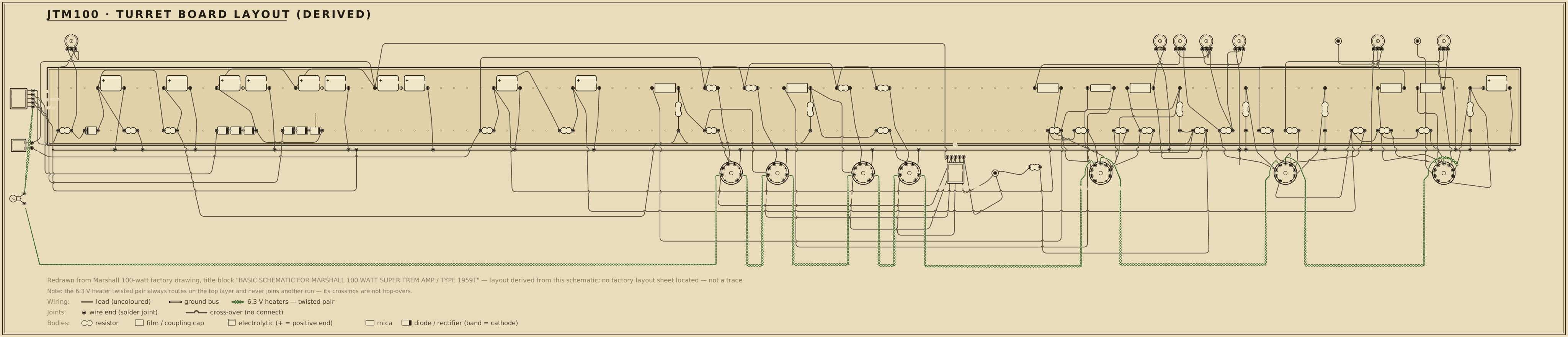
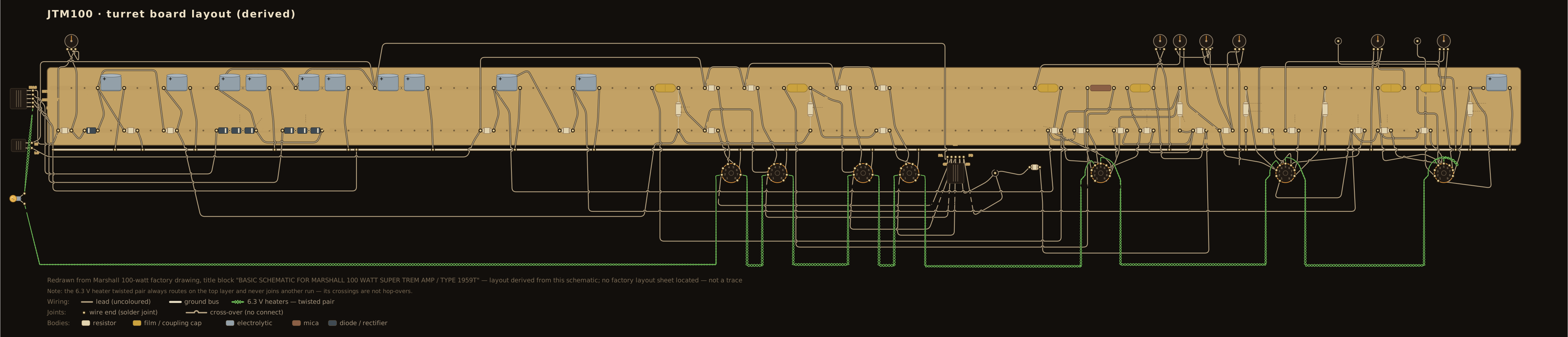
Board layout — redrawn reference diagram · source noted on the drawing Print sheet ↗
JTM100 turret board layout — an original diagram reconstructed from the redrawn schematic (no factory layout sheet exists), showing the principal parts in board order, drawn in the period layout-sheet style with each value lettered on the part.

Scroll the drawing sideways to read the whole board — the source line and the colour legend run along the bottom of the sheet — or open the full-size diagram in its own tab. Values are lettered on the parts in the period shorthand — .02-400, 250-5, 1MEG: how to read it.

Machine-checked wiring. Every modelled part the operating-point netlist places on this board has been verified in CI, terminal for terminal, to be electrically equivalent to the circuit's simulated netlist. This diagram documents connectivity and part arrangement — it is not a dimensioned 1:1 build template.

Details

The modelled parts are the tube sockets, the plate, cathode and grid-leak resistors, the power-rail droppers, and the coupling and bypass capacitors whose two leads are both named DC nodes; the check proves the same net structure, with no missing or extra connections. Parts outside that DC model — the volume / tone / mixer control-network internals, the negative-bias front end, and the heater chain, pilot lamp and power-transformer / rectifier AC side — are drawn from the cited sources but are not machine-checked; the CI report enumerates every one of their terminals so the boundary is explicit rather than silent.

Board and part positions are drawn at diagram scale, and lead dress, grounding paths, and physical spacing all matter in a high-voltage chassis. If you build from it, verify every connection against the schematic above and the operating-point table below as you go.
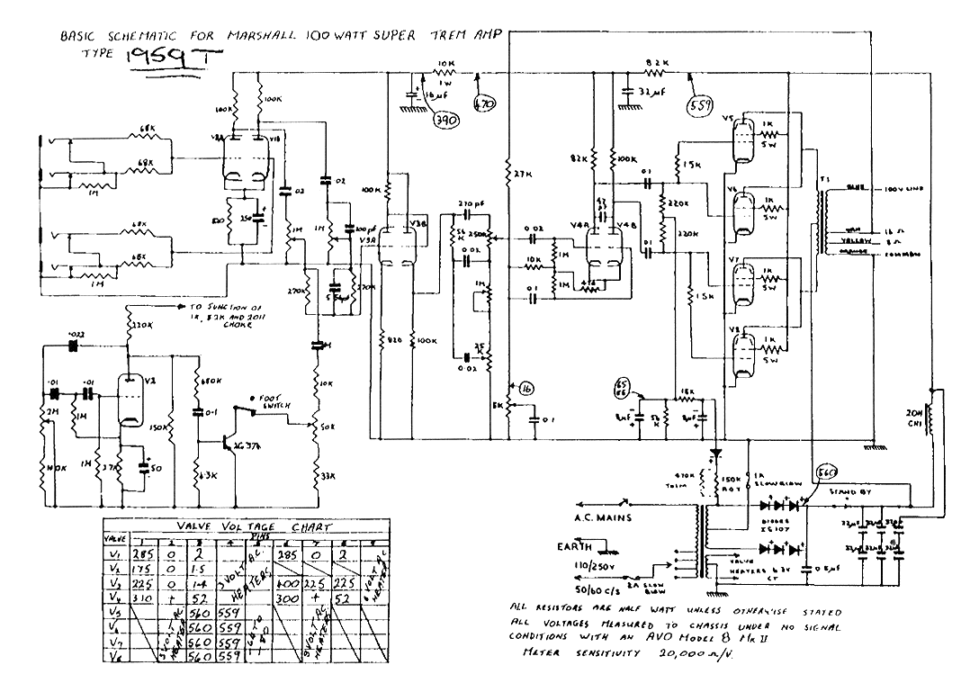
Operating point vs. published chart

Chart values read from the published drawing — or, where the drawing carries no voltage chart, from the cited published measurements (never reproduced). The simulated column is this circuit's own netlist solved in ngspice by the run that gates it; every deviation beside it is those two numbers compared, not a separately stated figure. Tolerances are this project's verification targets: tube-pin nodes carry the tolerance the cited source states, or ±20% — the era's printed convention — where it states none, and power rails are held to tighter internal targets.

Node Chart Simulated Deviation Tolerance Note
BP2 559 V 558.5 V 0.1% ±8% KT66 screen node after the 20 H choke (DCR estimated at 150 Ω, as in jtm45) — the drawing's circled 559 and the chart's V5–V8 pin-4 rows agree on it
BP3 470 V 473.8 V 0.8% ±8% phase-inverter rail after the 8.2 kΩ dropper — circled on the drawing
BP4 390 V 406.7 V 4.3% ±8% preamp rail after the 10 kΩ/1 W dropper — circled on the drawing. The chart's own V3 pin 6 reads 400 V at the cathode follower's plate, which is this same node; the two printed figures differ by 2.5%
P1A 285 V 275.0 V 3.5% ±20% ECC83 input plate, channel I (chart V1 pin 1)
P1B 285 V 275.0 V 3.5% ±20% ECC83 input plate, channel II (chart V1 pin 6)
KA 2 V 2.2 V 8.1% ±20% shared ECC83 input cathode, 820 Ω with a 25 µF bypass (chart V1 pins 3 and 8)
P3A 225 V 229.7 V 2.1% ±20% V3A plate = cathode-follower grid, direct-coupled (chart V3 pin 1, and pin 7 reads the same 225 at the follower's grid)
K3A 1.4 V 1.5 V 3.7% ±20% V3A cathode, 820 Ω unbypassed (chart V3 pin 3)
KCF 225 V 230.3 V 2.3% ±20% cathode-follower output over its 100 kΩ load (chart V3 pin 8)
PPIA 310 V 316.0 V 1.9% ±20% phase-inverter plate, 82 kΩ side — the tone-stack-driven triode (chart V4 pin 1)
PPIB 300 V 304.4 V 1.5% ±20% phase-inverter plate, 100 kΩ side (chart V4 pin 6)
KPI 52 V 56.0 V 7.7% ±20% phase-inverter cathodes, 470 Ω above the tail junction (chart V4 pins 3 and 8)
PRES 16 V 18.1 V 13.1% ±20% top of the 5 kΩ presence pot, where the 10 kΩ tail lands and the 27 kΩ feedback resistor arrives — circled on the drawing. Set by phase-inverter current, so it carries the tube-pin tolerance rather than the rail one
JPI 54.3 V tail junction where both 1 MΩ grid leaks return; the chart prints the phase-inverter grids only as '+' (qualitative)
S5 558.5 V V5 screen after its 1 kΩ/5 W stopper. The chart's 559 V pin-4 figure is already gated at BP2; this node is informational because the anchor-point KT66 model draws no screen current at this operating point (its screen term goes to zero below Vg2/mu + Vg1 = 0), so the stopper shows no drop and the node reads exactly BP2 — a v0-model limitation, models/METHODOLOGY.md
NGA −65.0 V phase-A output-grid node: the 0.1 µF coupler, the 220 kΩ leak to the bias line, V6's grid directly and V5's grid through its 15 kΩ stopper. The chart's pin-5 cell is an illegible hand-lettered range, so the modelled -65 V comes from the drawing's circled bias-filter figure instead
NGB −65.0 V phase-B output-grid node — V7 direct, V8 through its 15 kΩ stopper; same basis as NGA

Tube-pin nodes are checked at the tolerance the cited source states, or at the era's ±20% convention where it states none; power-rail nodes are held to tighter internal verification targets. Simulated figures are the netlist's DC solution, not measurements from a chassis.

The output stage behind these numbers can be drawn: the load line explorer plots this circuit's KT66 quartet at the DC operating point its netlist carries — 560 V on the plates with a −65 V grid bias — and marks where the load line crosses. This circuit is published as a draft, so that operating point is not verified against a published chart: the table and notes above say what each figure rests on.

Parts list

Every designator in this list appears on the schematic above, and every designator on the schematic appears here — the two are checked against each other in both directions, a valve's two halves counting as one bottle (V1A and V1B are both V1). Four parts the drawing carries as annotations rather than numbered symbols are listed here without designators, and stand outside that check. Valve numbers are the source drawing's own and are not renumbered here to close a gap: this circuit carries V1, V3, V4, V5, V6, V7 and V8, and a number missing from that run is a valve the circuit does not carry. This is the plain (non-tremolo) head read off the factory sheet for the tremolo version, the same relationship the corpus's jtm45 entry has with its drawing: the sheet's V2 tremolo valve, its transistor, and the depth network that shunts the V3A grid node are omitted, so the valve numbering follows the drawing and skips V2 (V1 input pair, V3 second stage + cathode follower, V4 phase inverter, V5-V8 the KT66 quartet). The schematic draws one jack per channel; the chassis carries four. Capacitor working voltages are NOT given: this drawing prints none for the signal-path parts, and the corpus does not invent ratings. The drawing's own footnote — "all resistors are half watt unless otherwise stated" — supplies the wattage for every resistor the sheet does not letter, including the 8.2 kOhm dropper. The factory sheet numbers almost nothing, so every designator here is the corpus's own; the only parts left without one are those no drawing in this entry places: the power transformer, the two mains/HT fuses and the capacitor paralleling the channel II mixer, whose value the archived scan does not render.

RefPartValue / ratingRole
R1s Carbon comp resistor 68 kΩ · ½ W Channel I grid stopper (one per jack; four on the chassis)
R2s Carbon comp resistor 68 kΩ · ½ W Channel II grid stopper
RG1 Carbon comp resistor 1 MΩ · ½ W Channel I input grid leak
RG2 Carbon comp resistor 1 MΩ · ½ W Channel II input grid leak
RL1 Carbon comp resistor 100 kΩ · ½ W V1A plate load
RL2 Carbon comp resistor 100 kΩ · ½ W V1B plate load
RK1 Carbon comp resistor 820 Ω · ½ W Shared ECC83 input cathode bias
C3 Electrolytic capacitor 25 µF Shared input cathode bypass
C1 Coupling capacitor 0.02 µF V1A → channel I volume
C2 Coupling capacitor 0.02 µF V1B → channel II volume
VR1 Audio-taper potentiometer 1 MΩ Channel I volume
VR2 Audio-taper potentiometer 1 MΩ Channel II volume
C23 Mica capacitor 100 pF Bright cap across the channel II volume (VR2)
RM1 Carbon comp resistor 270 kΩ · ½ W Channel I mixer
RM2 Carbon comp resistor 270 kΩ · ½ W Channel II mixer
RL3 Carbon comp resistor 100 kΩ · ½ W V3A plate load
RK2 Carbon comp resistor 820 Ω · ½ W V3A cathode bias (unbypassed on this sheet)
RKCF Carbon comp resistor 100 kΩ · ½ W Cathode-follower load
RSL Carbon comp resistor 56 kΩ · ½ W Tone-stack slope resistor
C4 Mica capacitor 270 pF Tone stack — treble
VR3 Potentiometer 250 kΩ Treble
C5 Film capacitor 0.02 µF Tone stack — bass
VR4 Audio-taper potentiometer 1 MΩ Bass
C6 Film capacitor 0.02 µF Tone stack — middle
VR5 Linear potentiometer 25 kΩ Middle
C7 Coupling capacitor 0.02 µF Tone stack → phase-inverter grid
RLA Carbon comp resistor 82 kΩ · ½ W PI plate load (V4A, tone-stack side)
RLB Carbon comp resistor 100 kΩ · ½ W PI plate load (V4B)
RGA Carbon comp resistor 1 MΩ · ½ W PI grid leak (V4A), returned to the tail junction
RGB Carbon comp resistor 1 MΩ · ½ W PI grid leak (V4B), returned to the tail junction
C8 Film capacitor 0.1 µF V4B grid AC-coupled to the presence/feedback node
C12 Mica capacitor 47 pF PI plate-to-plate phase compensation
RTAIL Carbon comp resistor 470 Ω · ½ W PI cathodes → tail junction
RT2 Carbon comp resistor 10 kΩ · ½ W PI tail, junction → presence pot
RNFB Carbon comp resistor 27 kΩ · ½ W Negative feedback, 16 Ω secondary tap → top of the presence pot
VR7 Linear potentiometer 5 kΩ Presence — in series in the phase-inverter tail, not shunting it to ground
C11 Film capacitor 0.1 µF Presence-pot wiper to ground
C9 Coupling capacitor 0.1 µF PI → phase-A output grids (V5/V6)
C10 Coupling capacitor 0.1 µF PI → phase-B output grids (V7/V8)
RGL1 Carbon comp resistor 220 kΩ · ½ W Phase-A output grid leak, from the bias line
RGL2 Carbon comp resistor 220 kΩ · ½ W Phase-B output grid leak, from the bias line
R5s Carbon comp resistor 15 kΩ · ½ W V5 grid stopper (the sheet gives V6's grid no stopper)
R8s Carbon comp resistor 15 kΩ · ½ W V8 grid stopper (the sheet gives V7's grid no stopper)
RS1 Carbon comp resistor 1 kΩ · 5 W V5 screen resistor
RS2 Carbon comp resistor 1 kΩ · 5 W V6 screen resistor
RS3 Carbon comp resistor 1 kΩ · 5 W V7 screen resistor
RS4 Carbon comp resistor 1 kΩ · 5 W V8 screen resistor
L1 Filter choke 20 H Reservoir → KT66 screen node
RD1 Carbon comp resistor 8.2 kΩ · ½ W Rail dropper, screens → phase inverter
RD2 Power resistor 10 kΩ · 1 W Rail dropper, phase inverter → preamp
C13 Electrolytic capacitor 32 µF HT reservoir, series pair 1 (upper)
C14 Electrolytic capacitor 32 µF HT reservoir, series pair 1 (lower)
C15 Electrolytic capacitor 32 µF HT reservoir, series pair 2 (upper)
C16 Electrolytic capacitor 32 µF HT reservoir, series pair 2 (lower)
C17 Electrolytic capacitor 32 µF HT reservoir, series pair 3 (upper)
C18 Electrolytic capacitor 32 µF HT reservoir, series pair 3 (lower)
C19 Electrolytic capacitor 32 µF Phase-inverter rail filter
C20 Electrolytic capacitor 16 µF Preamp rail filter
D1 Rectifier diode IS107 HT rectifier, arm A (three in series; the sheet letters them 'DIODES IS107')
D2 Rectifier diode IS107 HT rectifier, arm A (three in series; the sheet letters them 'DIODES IS107')
D3 Rectifier diode IS107 HT rectifier, arm A (three in series; the sheet letters them 'DIODES IS107')
D4 Rectifier diode IS107 HT rectifier, arm B (three in series; the sheet letters them 'DIODES IS107')
D5 Rectifier diode IS107 HT rectifier, arm B (three in series; the sheet letters them 'DIODES IS107')
D6 Rectifier diode IS107 HT rectifier, arm B (three in series; the sheet letters them 'DIODES IS107')
D7 Rectifier diode IS107 Bias supply rectifier
VR6 Trimmer potentiometer 470 kΩ Bias trim
RB1 Carbon comp resistor 150 kΩ · ½ W Bias supply series resistor
RB2 Carbon comp resistor 56 kΩ · ½ W Bias divider to ground
RB3 Carbon comp resistor 16 kΩ · ½ W Bias filter series resistor
C21 Electrolytic capacitor 8 µF Bias filter (supply side)
C22 Electrolytic capacitor 8 µF Bias filter (grid-line side)
V1 Preamp tube ECC83 (12AX7) Both input stages (V1A/V1B)
V3 Preamp tube ECC83 (12AX7) Second stage + cathode follower (V3A/V3B)
V4 Preamp tube ECC83 (12AX7) Long-tailed-pair phase inverter (V4A/V4B)
V5 Power tube KT66 Parallel push-pull output, phase A
V6 Power tube KT66 Parallel push-pull output, phase A
V7 Power tube KT66 Parallel push-pull output, phase B
V8 Power tube KT66 Parallel push-pull output, phase B
T1 Output transformer Push-pull, 4x KT66 primary Output to the speaker; secondary leads lettered on the sheet — blue 100 V line, white 16 Ω, yellow 8 Ω, orange common
Power transformer 110/250 V universal primary · HT + 6.3 V heaters HT and heater supply
Film capacitor value illegible on the archived scan Capacitor drawn in parallel with the channel II mixer RM2 (annotation only)
Fuse 2 A slow-blow Mains fuse
Fuse 1 A slow-blow HT centre-tap fuse

Circuit story

The head that doubled Marshall's output stage. Players wanted more volume on stage than 45 watts gave, and the answer was arithmetic rather than invention: take the JTM45, keep the front end almost untouched, and hang four KT66 beam tetrodes on a much stiffer supply. Nothing about the preamp announces the change — four jacks, two channels, a direct-coupled cathode follower feeding a treble-middle-bass stack, a long-tailed-pair inverter. Everything after the inverter is new: two output valves become four, the GZ34 rectifier valve disappears in favour of silicon, and the plate rail climbs from the JTM45's 450 V to 560 V.

That last number is the character of the amplifier and also its reputation. A KT66 is rated for 25 W of plate dissipation; at 560 V there is very little room between a usable idle current and the rating, which is one reason the 100-watt heads moved to EL34s and then to lower rails within a couple of years. The amplifier documented here is the KT66 window: 1965 into 1966, the era of left-over JTM45 front panels on 100-watt chassis that gave these heads their other common name, JTM45/100.

Circuit walkthrough (short form)

Four jacks across two channels (1 MΩ leaks, 68 kΩ stoppers) → V1 ECC83 (100 kΩ plates, one shared 820 Ω cathode with a 25 µF bypass) → 0.02 µF couplers → 1 MΩ volume pots (100 pF bright cap across the second) → 270 kΩ mixers → V3A ECC83 (100 kΩ plate, unbypassed 820 Ω cathode) → V3B cathode follower, DC-coupled (100 kΩ load) → TMB stack (56 kΩ slope; 270 pF, 0.02 µF and 0.02 µF; 250 kΩ / 1 MΩ / 25 kΩ pots) → 0.02 µF → long-tailed-pair PI: 82 kΩ and 100 kΩ plates, 47 pF across them, 470 Ω from the joined cathodes to the tail junction where both 1 MΩ leaks return, then 10 kΩ down to the presence pot → 0.1 µF couplers onto two phase nodes, each with a 220 kΩ grid leak to the bias line → four KT66s, 1 kΩ · 5 W screen stoppers on all four → output transformer, whose secondary leads the sheet letters by colour — blue for a 100 V line tap, white 16 Ω, yellow 8 Ω, orange common — with 27 kΩ of negative feedback from the 16 Ω tap.

Power: a universal-primary mains transformer (110/250 V), two arms of three series silicon diodes and a standby switch into a reservoir of three series 32 µF pairs — a 2 A slow-blow fuse in the mains lead, a 1 A slow-blow in the HT centre-tap return — 560 V, feeding the output plates through the transformer primary. A 20 H choke takes that to the 559 V screen node; 8.2 kΩ and a 32 µF drop to the 470 V inverter rail; 10 kΩ · 1 W and 16 µF drop again to the 390 V preamp rail. The negative grid bias has its own diode, a 470 kΩ trim, 150 kΩ, a 56 kΩ / 16 kΩ divider and two 8 µF filters, and the drawing circles −65/−66 V at it.

Two things the drawing does that a tidy redrawing would not

The presence control sits inside the tail, not beside it. On the JTM45 the inverter's 10 kΩ tail goes to ground and the presence pot and feedback resistor join it there. Here the 10 kΩ lands on the top of the 5 kΩ presence pot, and the pot completes the path to ground. The chart proves it rather than merely allowing it: 52 V at the inverter cathodes with 310 V and 300 V plates off a 470 V rail means 3.65 mA in the tail, which needs about 14 kΩ to ground — the 10 kΩ alone would put the cathodes near 37 V. The drawing then circles 16 V at the pot's top, which is what 3.65 mA through 5 kΩ gives. Three independently printed numbers agree on one topology.

That node is also where the feedback arrives and where the inverter's second grid is driven from: the 27 kΩ comes down to it from the 16 Ω tap, and a 0.1 µF couples it up to the V4B grid. The two 1 MΩ grid leaks return not there but to the junction between themselves, one 10 kΩ further up the tail — a distinction the sheet draws plainly and a redrawing can easily lose.

Only half the output valves get a grid stopper. Each phase node feeds one valve through a 15 kΩ stopper and the other valve's grid directly off the node — V5 and V8 stoppered, V6 and V7 not. That is what the sheet draws, at every zoom level, and it is reproduced rather than symmetrised. It costs nothing at DC (no grid current, so all four grids sit on the bias line either way) and it is exactly the sort of detail a redrawing quietly "fixes" into something the factory never built.

Lineage

The JTM100 is the JTM45 with its output section doubled, and through the JTM45 it descends from the tweed 5F6-A Bassman. Forward, it is the circuit Marshall catalogued as the 1959 Super Lead: the corpus's m1959 entry documents the July-1970 factory drawing of that model, by which point the KT66 quartet had become four EL34s and the choke-and-dropper supply had been rearranged. The 100-watt line's 50-watt sibling took the same path from JTM50 to the model 1987.

The tone network, as the drawing wires it

The stack is the JTM45's, one component value apart: 56 kΩ slope resistor, 270 pF across the treble pot, 250 kΩ treble, 1 MΩ bass, 25 kΩ middle. Where the JTM45 uses 0.01 µF for the middle cap this sheet letters 0.02 µF, so both the bass and middle caps read the same value. The later cataloged 1959 drawing replaces the whole front of the stack with 500 pF and 33 kΩ; that change is not in this sheet.

Verification — against the printed factory chart

This drawing prints a full VALVE VOLTAGE CHART, measured "to chassis under no signal conditions with an AVO Model 8 Mk II, meter sensitivity 20,000 Ω/V", and it circles six further node voltages on the schematic itself. That is a richer measurement basis than any other Marshall sheet in the corpus, and the circuit reproduces it well: every rail lands within 4.3% of its circled figure, every preamp and inverter plate within 3.5%, and all three hand-meter cathode readings within 8%. The worst node is the presence-pot top at 13.1% — a single-digit reading set by tube current rather than by a stiff supply.

The entry is nonetheless published as a draft, for two reasons that have nothing to do with the chart.

The first is the output stage. The v0 KT66 model is an anchor-point fit taken at 250 V (models/METHODOLOGY.md); this circuit runs its screens at 559 V, and at that operating point the model idles each valve near 72 mA — about 40 W against the KT66's published 25 W rating. Real amplifiers of this type are set far colder. Nothing in the gated node set depends on that current (the model draws no screen current here at all, so the 1 kΩ stoppers show no drop and the screen nodes read exactly the rail), but a circuit whose output valves simulate at 160% of their rating is not one to stamp verified.

The second is the chart's own two silent cells. The inverter grids are printed as "+" rather than a number, and the KT66 control-grid cell is a hand-lettered range that the archived scan does not render legibly, so the modelled bias comes from the schematic's circled −65/−66 V instead of from the chart. Both nodes are reported informationally rather than gated.

A naming note

The title block reads "BASIC SCHEMATIC FOR MARSHALL 100 WATT SUPER TREM AMP / TYPE 1959T", and it is the tremolo version of the head — the same relationship the corpus's jtm45 entry has to its own factory sheet, which is likewise a trem drawing read for the plain head. The sheet's V2 tremolo valve and the transistor-driven depth network that shunts the V3A grid node are omitted here, which is why the valve numbering skips from V1 to V3. The circuit is filed under the era designation the schematic archives use for the 1965–67 100-watt heads, JTM100, because the bare 1959 designation belongs to the cataloged EL34 head already documented at m1959 and the two are different circuits.

Sources