M1959 Super Lead 100‑style · 1965–1981 · 100 W

draft
Schematic — redrawn in KiCad · scroll to zoom, drag to pan
Board layout — redrawn reference diagram · source noted on the drawing Print sheet ↗
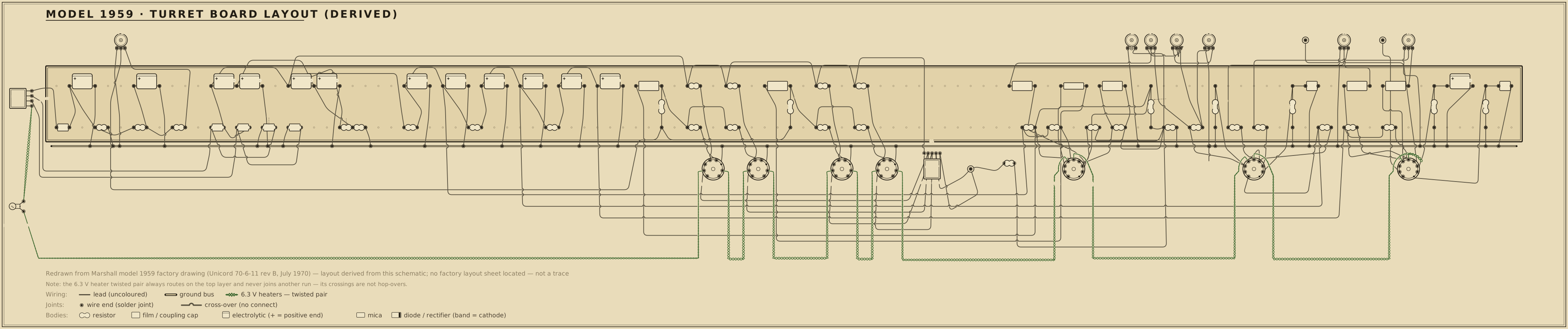
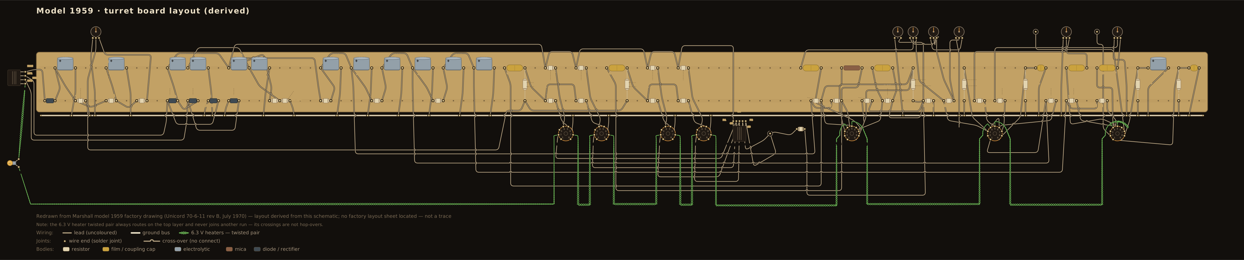
M1959 turret board layout — an original diagram reconstructed from the redrawn schematic (no factory layout sheet exists), showing the principal parts in board order, drawn in the period layout-sheet style with each value lettered on the part.

Scroll the drawing sideways to read the whole board — the source line and the colour legend run along the bottom of the sheet — or open the full-size diagram in its own tab. Values are lettered on the parts in the period shorthand — .02-400, 250-5, 1MEG: how to read it.

Machine-checked wiring. Every modelled part the operating-point netlist places on this board has been verified in CI, terminal for terminal, to be electrically equivalent to the circuit's simulated netlist. This diagram documents connectivity and part arrangement — it is not a dimensioned 1:1 build template.

Details

The modelled parts are the tube sockets, the plate, cathode and grid-leak resistors, the power-rail droppers, and the coupling and bypass capacitors whose two leads are both named DC nodes; the check proves the same net structure, with no missing or extra connections. Parts outside that DC model — the volume / tone / mixer control-network internals, the negative-bias front end, and the heater chain, pilot lamp and power-transformer / rectifier AC side — are drawn from the cited sources but are not machine-checked; the CI report enumerates every one of their terminals so the boundary is explicit rather than silent.

Board and part positions are drawn at diagram scale, and lead dress, grounding paths, and physical spacing all matter in a high-voltage chassis. If you build from it, verify every connection against the schematic above and the operating-point table below as you go.

Operating point vs. published chart

Chart values read from the published drawing — or, where the drawing carries no voltage chart, from the cited published measurements (never reproduced). The simulated column is this circuit's own netlist solved in ngspice by the run that gates it; every deviation beside it is those two numbers compared, not a separately stated figure. Tolerances are this project's verification targets: tube-pin nodes carry the tolerance the cited source states, or ±20% — the era's printed convention — where it states none, and power rails are held to tighter internal targets.

Node Chart Simulated Deviation Tolerance Note
P1A 135 V 141.1 V 4.5% ±20% V1A plate — channel I (high-treble) input, 100 kΩ load, 820 Ω cathode (chart V1 pin 1)
K1A 1 V 0.9 V 9.3% ±20% V1A cathode (820 Ω, 250 µF bypass) — chart V1 pin 3
P1B 195 V 187.0 V 4.1% ±20% V1B plate — channel II (normal) input, 100 kΩ load (chart V1 pin 6)
K1B 1.5 V 1.7 V 16.6% ±20% V1B cathode (2.7 kΩ, 0.68 µF partial bypass) — the colder channel; chart V1 pin 8
P2A 153 V 151.2 V 1.2% ±20% V2A plate — second gain stage (100 kΩ load), DC-coupled to the cathode follower; chart V2 pin 1
K2A 1.1 V 1.0 V 12.0% ±20% V2A cathode — chart V2 pin 3. The chart amp carries the 1 kΩ cathode resistor the drawing annotates as a variant; the netlist uses the drawing's primary 820 Ω, which idles this stage slightly hotter.
KCF 153 V 151.5 V 1.0% ±20% V2B cathode-follower output over its 100 kΩ load, feeding the TMB tone stack (chart V2 pin 8)
PPIA 210 V 204.7 V 2.5% ±20% phase-inverter plate, 82 kΩ side (V3A, driven from the tone stack); chart V3 pin 1
PPIB 195 V 195.7 V 0.3% ±20% phase-inverter plate, 100 kΩ side (V3B, the AC-grounded side); chart V3 pin 6
KPI 18.5 V 26.3 V 42.1% ±20% phase-inverter shared cathode above the 470 Ω (chart V3 pins 3 and 8). The simulated value runs high: the anchor-point 12AX7 model idles this pair at ~2.5 mA against the chart's 1.8 mA, and the supply it hangs on is itself high for the same reason.
BP2 313.8 V phase-inverter supply node, after the 20 kΩ/1 W dropper — no chart pin. The chart's own stage currents put it near 300 V
BP3 260 V 269.3 V 3.6% ±20% second-stage / cathode-follower supply node after the first 10 kΩ/1 W dropper — read from the cathode follower's plate, chart V2 pin 6
BP4 251.8 V input-stage supply node after the second 10 kΩ/1 W dropper — no chart pin; the chart's V1 plate and cathode figures put it near 254 V
JPI 25.1 V phase-inverter tail junction between the 470 Ω and the 10 kΩ, where both 1 MΩ grid leaks return
SG4 453.0 V V4 screen grid after its 1 kΩ stopper — the only published figure is the 6550 variant's 450 V. The anchor-point EL34 model draws no screen current at this operating point, so the simulated node sits exactly at B+1
G4 −46.0 V V4 control grid, fed from the adjustable bias supply through the 120 kΩ leak and a 5.6 kΩ stopper — the drawing prints no bias figure and the only published one is the 6550 variant's -51 V

Tube-pin nodes are checked at the tolerance the cited source states, or at the era's ±20% convention where it states none; power-rail nodes are held to tighter internal verification targets. Simulated figures are the netlist's DC solution, not measurements from a chassis.

The output stage behind these numbers can be drawn: the load line explorer plots this circuit's EL34 quartet at the DC operating point its netlist carries — 453 V on the plates with a −46 V grid bias — and marks where the load line crosses. This circuit is published as a draft, so that operating point is not verified against a published chart: the table and notes above say what each figure rests on.

Parts list

Every designator in this list appears on the schematic above, and every designator on the schematic appears here — the two are checked against each other in both directions, a valve's two halves counting as one bottle (V1A and V1B are both V1). Five parts the drawing carries as annotations rather than numbered symbols are listed here without designators, and stand outside that check. Cathode-bypass and coupling capacitor VALUES are open at DC and do not enter the operating-point netlist; they are listed for completeness. Where the drawing prints a second value in parentheses, that is a factory-annotated alternate: the primary value is listed and the alternate is named in the part's role. The HT-winding snubbers, the mains-to-chassis capacitor, the fuses, the standby switch and the pilot lamp are annotations on the factory sheet: the capacitors appear on the schematic without connections, and the rest carry no designator. The output transformer is the one transformer the list numbers — T1; the mains/HT transformer is drawn as an annotation and is listed without a designator.

RefPartValue / ratingRole
R1s Carbon comp resistor 68 kΩ · ½ W Channel I high-treble input grid stopper
R2s Carbon comp resistor 68 kΩ · ½ W Channel I normal input grid stopper
R3s Carbon comp resistor 68 kΩ · ½ W Channel II high input grid stopper
R4s Carbon comp resistor 68 kΩ · ½ W Channel II low input grid stopper
RG1 Carbon comp resistor 1 MΩ · ½ W Channel I input grid leak
RG2 Carbon comp resistor 1 MΩ · ½ W Channel II input grid leak
RL1 Carbon comp resistor 100 kΩ · ½ W V1A plate load (channel I)
RL2 Carbon comp resistor 100 kΩ · ½ W V1B plate load (channel II)
RK1 Carbon comp resistor 820 Ω · ½ W V1A cathode bias (channel I)
C1 Electrolytic capacitor 250 µF · 6 V V1A cathode bypass
RK2 Carbon comp resistor 2.7 kΩ · ½ W V1B cathode bias (channel II — the colder channel)
C2 Film capacitor 0.68 µF V1B cathode bypass (partial)
C3 Coupling capacitor 0.022 µF · 400 V V1A → channel I volume
C4 Coupling capacitor 0.0022 µF · 400 V V1B → channel II volume
VR1 Audio-taper potentiometer 1 MΩ Channel I (high-treble) volume
VR2 Audio-taper potentiometer 1 MΩ Channel II (normal) volume
C5 Film capacitor 0.005 µF Channel I bright/treble-bleed cap across the volume
C6 Mica capacitor 500 pF Channel II bright cap across the volume
RM1 Carbon comp resistor 470 kΩ · ½ W Channel I mixing resistor into V2A grid
RM2 Carbon comp resistor 470 kΩ · ½ W Channel II mixing resistor into V2A grid
RL3 Carbon comp resistor 100 kΩ · ½ W V2A plate load (second stage)
RK3 Carbon comp resistor 820 Ω · ½ W V2A cathode bias (drawing annotates a 1 kΩ variant; the published voltage chart's amp carries the 1 kΩ)
C7 Film capacitor 0.68 µF V2A cathode bypass (partial)
RKCF Carbon comp resistor 100 kΩ · ½ W V2B cathode-follower load
RSL Carbon comp resistor 33 kΩ · ½ W Tone-stack slope resistor
C8 Mica capacitor 500 pF Tone stack — treble
VR3 Potentiometer 250 kΩ Treble
C9 Film capacitor 0.022 µF · 400 V Tone stack — bass
VR4 Audio-taper potentiometer 1 MΩ Bass
C10 Film capacitor 0.022 µF · 400 V Tone stack — middle
VR5 Linear potentiometer 25 kΩ Middle
C11 Coupling capacitor 0.022 µF · 400 V Tone stack → phase-inverter grid
RGA Carbon comp resistor 1 MΩ · ½ W PI grid leak (V3A), returned to the tail junction
RGB Carbon comp resistor 1 MΩ · ½ W PI grid leak (V3B), returned to the tail junction
RLA Carbon comp resistor 82 kΩ · ½ W PI plate load (V3A, the tone-stack-driven side)
RLB Carbon comp resistor 100 kΩ · ½ W PI plate load (V3B)
RTAIL Carbon comp resistor 470 Ω · ½ W PI tail (shared cathode → junction)
RT2 Carbon comp resistor 10 kΩ · ½ W PI tail (junction → presence/feedback node)
C12 Mica capacitor 47 pF PI plate-to-plate / phase compensation
RNFB Carbon comp resistor 47 kΩ · ½ W Negative feedback, 16 Ω secondary tap → PI tail cold end (drawing annotates a 100 kΩ variant)
VR6 Linear potentiometer 5 kΩ Presence
C13 Film capacitor 0.1 µF Presence-pot wiper to ground
C14 Film capacitor 0.1 µF AC coupling from the presence/feedback node to the V3B grid
C15 Coupling capacitor 0.022 µF · 400 V PI (82 kΩ plate) → V4/V5 grid line
C16 Coupling capacitor 0.022 µF · 400 V PI (100 kΩ plate) → V6/V7 grid line
RGL1 Carbon comp resistor 120 kΩ · ½ W Grid leak for the V4/V5 pair, from the bias line
RGL2 Carbon comp resistor 120 kΩ · ½ W Grid leak for the V6/V7 pair, from the bias line
RS4 Carbon comp resistor 5.6 kΩ · ½ W V4 grid stopper
RS5 Carbon comp resistor 5.6 kΩ · ½ W V5 grid stopper
RS6 Carbon comp resistor 5.6 kΩ · ½ W V6 grid stopper
RS7 Carbon comp resistor 5.6 kΩ · ½ W V7 grid stopper
RSC4 Carbon comp resistor 1 kΩ V4 screen-grid stopper
RSC5 Carbon comp resistor 1 kΩ V5 screen-grid stopper
RSC6 Carbon comp resistor 1 kΩ V6 screen-grid stopper
RSC7 Carbon comp resistor 1 kΩ V7 screen-grid stopper
D1 Silicon rectifier diode 1008 Bias-supply rectifier — its own HT-tap diode
RBA Carbon comp resistor 27 kΩ · ½ W Bias-supply shunt at the diode (drawing annotates a 22 kΩ variant)
RBB Carbon comp resistor 15 kΩ · ½ W Bias-supply series resistor between the two 8 µF filters
RBC Carbon comp resistor 47 kΩ · ½ W Bias-adjust divider, upper leg
VR7 Trim potentiometer 27 kΩ Bias adjust
C17 Electrolytic capacitor 8 µF Bias-supply filter
C18 Electrolytic capacitor 8 µF Bias-supply filter
RD1 Power resistor 20 kΩ · 1 W Rail dropper B+1 (reservoir / screens) → B+2 (phase inverter)
RD2 Power resistor 10 kΩ · 1 W Rail dropper B+2 (phase inverter) → B+3 (second stage / cathode follower)
RD3 Power resistor 10 kΩ · 1 W Rail dropper B+3 (second stage) → B+4 (input stage)
C19 Electrolytic capacitor 100 µF · 350 V Reservoir filter, upper half of a series pair
C20 Electrolytic capacitor 100 µF · 350 V Reservoir filter, lower half of a series pair
C21 Electrolytic capacitor 100 µF · 350 V Second reservoir bank, upper half of a series pair
C22 Electrolytic capacitor 100 µF · 350 V Second reservoir bank, lower half of a series pair
RB1 Carbon comp resistor 56 kΩ Voltage-sharing resistor across a series reservoir capacitor
RB2 Carbon comp resistor 56 kΩ Voltage-sharing resistor across a series reservoir capacitor
C23 Electrolytic capacitor 50 µF · 350 V Phase-inverter-supply filter
C24 Electrolytic capacitor 50 µF · 350 V Phase-inverter-supply filter
C25 Electrolytic capacitor 50 µF · 350 V Second-stage-supply filter
C26 Electrolytic capacitor 50 µF · 350 V Second-stage-supply filter
C27 Electrolytic capacitor 50 µF · 350 V Input-stage-supply filter
C28 Electrolytic capacitor 50 µF · 350 V Input-stage-supply filter
D2 Silicon rectifier diode A10D10 HT bridge rectifier arm
D3 Silicon rectifier diode A10D10 HT bridge rectifier arm
D4 Silicon rectifier diode A10D10 HT bridge rectifier arm
D5 Silicon rectifier diode A10D10 HT bridge rectifier arm
C29 Film capacitor 0.22 µF HT-winding snubber
C30 Film capacitor 0.22 µF HT-winding snubber
C31 Film capacitor 0.05 µF Mains line-to-chassis capacitor
V1 Preamp tube ECC83 (12AX7) Input valve — both channels (V1A/V1B)
V2 Preamp tube ECC83 (12AX7) Second stage + cathode follower (V2A/V2B)
V3 Preamp tube ECC83 (12AX7) Long-tailed-pair phase inverter (V3A/V3B)
V4 Power tube EL34 Parallel push-pull output — phase A
V5 Power tube EL34 Parallel push-pull output — phase A
V6 Power tube EL34 Parallel push-pull output — phase B
V7 Power tube EL34 Parallel push-pull output — phase B
T1 Output transformer 16/8/4 Ω taps Output transformer — parallel push-pull primary for four EL34s, 16/8/4 Ω secondary taps (feedback from the 16 Ω tap)
Power transformer Universal primary 110/120/200/225/245 V · HT + 6.3 V heaters Mains/HT transformer
Fuse 4 A Mains fuse (annotation)
Fuse 1 A HT fuse (annotation)
Standby switch SPST HT standby (annotation)
Pilot lamp 6.3 V Panel pilot lamp (annotation)

Circuit story

The Marshall model 1959 is the 100-watt Super Lead: the amplifier most people mean when they say "Plexi". It began as a special order — 100-watt heads built for players who wanted more than the 45-watt amplifier could give them on stage — and became Marshall's catalogue number 1959, produced from 1965 until 1981.

The signal path is the one the whole lead line shares — the 50-watt model 1987 carries the same one two years later. Four inputs feed two deliberately unmatched channels into one ECC83; a second ECC83 provides a gain stage and a direct-coupled cathode follower ahead of the treble-middle-bass tone stack; a third drives a long-tailed-pair phase inverter. What changes at 100 watts is behind the inverter: four EL34 pentodes in parallel push-pull, two per phase, over a solid-state bridge rectifier and a filter bank of paired 100 µF capacitors. There is no rectifier valve to sag, and there is a great deal of power supply behind the output valves, which is much of why the 1959 stays tight and loud where smaller amplifiers compress.

"Plexi" names the circuit and its voicing, not the panel: Marshall switched from the gold acrylic (Perspex) front panel to a brushed-metal panel around 1969, so the factory drawing cited here (Unicord, July 1970) is metal-panel era.

Circuit walkthrough (short form)

Two channels, each with high and low inputs (68 kΩ stoppers, 1 MΩ leaks) → V1 ECC83, one triode per channel (100 kΩ plates). The channels are voiced apart at the cathode: the high-treble channel runs 820 Ω fully bypassed by 250 µF, the normal channel a colder 2.7 kΩ with a 0.68 µF partial bypass, and their coupling caps differ too (0.022 µF and 0.0022 µF). Each plate feeds its own 1 MΩ volume with a bright cap (0.005 µF and 500 pF), and the two channels mix through 470 kΩ resistors into V2A (100 kΩ plate, 820 Ω / 0.68 µF cathode) → V2B cathode follower, DC-coupled (100 kΩ load) → tone stack (33 kΩ slope; 500 pF treble into 250 kΩ, 0.022 µF bass into 1 MΩ, 0.022 µF middle into 25 kΩ) → long-tailed-pair phase inverter (V3: 82 kΩ plate on the driven side and 100 kΩ on the other, 470 Ω over a 10 kΩ tail, both 1 MΩ grid leaks returned to the tail junction, 47 pF across the plates).

From there the two phases split: each 0.022 µF coupler feeds a pair of EL34s through 5.6 kΩ grid stoppers, with one 120 kΩ grid leak per pair carrying the adjustable negative bias. Every screen grid has its own 1 kΩ stopper. The output transformer offers 16, 8 and 4 Ω taps, and negative feedback returns from the 16 Ω tap through a 47 kΩ resistor to the cold end of the inverter's tail, where a 5 kΩ presence control shunts the top of the feedback band to ground.

Power: a universal-primary mains transformer (110/120/200/225/245 V taps), a silicon bridge and a reservoir of 100 µF capacitors in series pairs with 56 kΩ sharing resistors. That rail feeds the output valves' plates and screens directly; a 20 kΩ / 1 W dropper takes it down to the phase inverter and two further 10 kΩ / 1 W droppers step it down again for the second stage and the input valve, each node filtered by a pair of 50 µF capacitors. The negative grid bias comes from its own diode, a 15 kΩ / 27 kΩ / 47 kΩ network with 8 µF filters and a 27 kΩ trimmer.

Lineage

The 1959 descends from the JTM45, and through it from the tweed 5F6-A Bassman the JTM45 copied. The path runs through the 100-watt heads Marshall built in 1965 for players who wanted more clean headroom than 45 watts gave: the output section was doubled, and the KT66 beam tetrodes gave way to EL34 pentodes as KT66 costs rose. The valve rectifier went with them. The front end barely moved — four inputs, two channels, a DC-coupled cathode follower and a long-tailed-pair inverter all carry straight across from the JTM45.

The 50-watt model 1987 is this amplifier's sibling rather than its parent: the same front end and the same voicing with half the output valves.

The tone network, as the drawing wires it

The Unicord drawing wires the stack identically to the model 1987's, wire for wire: 500 pF and the 33 kΩ slope off the cathode-follower output; 0.022 µF from the slope foot to the treble pot's lower lug and the bass pot; the bass pot a rheostat in series down the ladder; 0.022 µF into the middle pot's wiper; output from the treble pot's wiper alone. The schematic, the board diagram and the tone-stack lab all follow the drawing rather than the textbook redrawing that joins the two wipers.

A note on verification

Marshall drawings of this period print component values only, and the 1959 drawing carries no valve-voltage chart. A factory chart does exist for the 100-watt head, issued with the sheet of the same drawing number and date that covers the 6550-fitted Mark II — a component-for-component identical front end ahead of a different output quartet. Its ECC83 figures are used here for the preamp and phase inverter, and the circuit reproduces them closely: every preamp plate lands within 5% of its printed figure and the inverter's two plates within 3%. The cathode figures — single-digit-volt readings taken with a hand-held meter — land within 17%.

Two things keep the circuit a draft. The inverter's cathode simulates about 8 volts above the printed figure, because the model idles that pair harder than the chart's amplifier did and the supply it hangs on runs high for the same reason. And the EL34 output stage has no published figures of its own at all: its plate and screen voltages here are derived from a rail taken as an assumption, and the idle current is a choice within the range these amplifiers are set to rather than a reading. Verified is earned against measurements, and the measurements that exist do not cover this output stage.

Sources