The 4×10, 6L6GC step up from the Deluxe Reverb: a 40-watt combo running the
same reverb-and-tremolo Vibrato channel as its blackface siblings, but on a
bigger power section and — as printed on its own schematic — a genuinely
asymmetric pair of tone stacks. The blackface Super Reverb ships under the
AA763 drawing from 1963 and moves to the AB763 revision below for the rest of
its run, 1964 to 1967. Two channels feed the shared output stage: a plain
Normal channel and a Vibrato channel carrying the reverb and the
tremolo, into a fixed-biased 6L6GC pair through a 12AT7 phase inverter,
rectified by a GZ34. The preamp bottles are marked 7025 on the drawing,
the low-noise selected version of the 12AX7; the tremolo oscillator is
labelled plain 12AX7; the reverb driver and phase inverter are 12AT7s.
Signal path
Normal channel. Two inputs (68 kΩ stoppers into the grid, with the 1 MΩ
leak at input 1's tip, jack side of its stopper) → a 12AX7 stage (100 kΩ plate load, 1.5 kΩ cathode with a 25 µF bypass) → a
two-knob tone stack — Treble and Bass only, the middle leg tied to a fixed
6.8 kΩ bleed resistor rather than a control — and a 1 MΩ volume with its own
120 pF bright switch → a second 12AX7 stage (100 kΩ plate; its cathode
carries no resistor of its own — see Two cathode networks, four triodes
below) → a 0.047 µF coupling cap and a 220 kΩ mixing resistor to the junction
that feeds the phase inverter. No reverb, no tremolo.
Vibrato channel. Input stage as above → a three-knob tone stack —
Treble, Bass, and Middle, where the Normal channel's fixed bleed resistor
is replaced by a genuine 10 kΩ-A potentiometer — and its own 120 pF bright
switch → a second 12AX7 stage (100 kΩ plate, on the 820 Ω cathode network it
shares with the Normal channel's second stage). Its 0.02 µF coupler feeds a dry
node with two branches: a 500 pF cap to the reverb driver, and a 3.3 MΩ
resistor (10 pF across it) into the mix driver's grid.
Two tone stacks on one chassis
The two tone stacks are not the same circuit with a knob added — the Normal
channel's middle leg is hard-wired to ground through 6.8 kΩ, full stop, while
the Vibrato channel's is a control a player turns. This is read directly off
the schematic, not inferred from the panel layout. The Middle pot itself is an
ordinary 10 kΩ audio-taper part, the same value the Twin
Reverb fits; what is unusual is having it on one channel
and a fixed resistor on the other, on one chassis.
That leaves this circuit straddling a distinction the corpus's topology field
draws in one value. The field names the Vibrato channel — a full FMV stack,
which is what a player means by a Super Reverb, and which puts this amp beside
the Twin rather than beside the two-knob
Deluxe Reverb on the tone-stack cross-cut. The Normal channel's
fixed bleed is the exception, and it is documented here rather than averaged
away. Until 2026-09-09 the field said treble/bass, which contradicted this
circuit's own parts list.
Reverb. The dry Vibrato signal drives a 12AT7 with both triodes in
parallel (2.2 kΩ shared cathode) into the 125A20B transformer and the
spring tank — the same reverb-transformer part number the Deluxe Reverb and
Twin Reverb entries in this corpus cite. The returned signal comes back
through a 12AX7 recovery stage (100 kΩ plate, 820 Ω cathode; the tank's output lands on
the grid, which a 220 kΩ leak returns to ground), is set by the 100 kΩ Reverb control, and returns through
470 kΩ onto the mix driver's grid.
Tremolo. The tremolo tube is a 12AX7 doing two jobs. One triode is a
phase-shift oscillator (220 kΩ plate load, 2.7 kΩ cathode). Its ladder runs from
the plate through 0.02 µF to the Speed node — a 3 MΩ reverse-audio Speed control
and 100 kΩ to ground — then through 0.01 µF to a middle node and another
0.01 µF to the grid. A 1 MΩ from the middle node and another from the grid meet
at the footswitch junction, which returns through 2.2 MΩ to the bias supply's
filter node. The other triode takes its grid from that middle node and drives
the neon lamp of an optocoupler: the lamp sits between its plate and a
100 kΩ feed from the +460 V rail, with a 10 MΩ bleeder beside it and a 100 kΩ
cathode resistor. The lamp faces a photoresistor that shunts the wiper of the
50 kΩ reverse-audio Intensity control to ground, and that control hangs from
the mix driver's output, between its 0.1 µF coupler and its 220 kΩ mixing
resistor, so the tremolo swings the Vibrato channel's level on its way to the
phase inverter.
Mix driver and phase inverter. A third 12AX7 stage (100 kΩ plate, 820 Ω
cathode) sums the two: the dry signal reaches its grid through 3.3 MΩ with
10 pF across it, the recovered reverb through 470 kΩ, and a 220 kΩ leak holds
the grid at ground. Its output runs through 0.1 µF (the node the Intensity
control hangs from) and a 220 kΩ mixing resistor to the junction the Normal
channel's own 220 kΩ reaches, and 0.001 µF carries the sum to a 12AT7
long-tailed pair (82 kΩ and 100 kΩ 5% plate loads, a 470 Ω cathode
resistor to a tail junction, both 1 MΩ grid leaks returned to that
junction, and a 22 kΩ tail from it to the feedback node, which a 100 Ω
returns to ground) — exactly the tail values the Deluxe
Reverb's own phase inverter uses. The pair splits the signal for the 6L6GC pair, each output
tube fixed-biased at −52 V through a 220 kΩ leak and its own 1.5 kΩ grid
stopper — a resistor the Deluxe Reverb's 6V6GT stage does not carry — with
470 Ω · 1 W screen resistors, and an 820 Ω negative-feedback resistor returning
from the speaker to that same feedback node.
Power
360-0-360 V (power transformer 125P5D) → GZ34 → a series pair of 70 µF · 350 V
reservoir caps after the standby switch (each with a 220 kΩ balancing
resistor across it) →
filter choke (125C1A) → +460 V at the 6L6GC plates (the output
transformer 125A9A's centre tap reads +465 V on the chart, 5 V above the
plate reading — merged to one modelled rail, the primary DCR omitted, exactly
as the Deluxe Reverb merges its own +415 V/+420 V pair) → +460 V screens (via
470 Ω · 1 W stoppers) → a printed 1 kΩ dropper → +450 V at the
phase-inverter plates and the reverb-driver plate → a printed 4.7 kΩ
dropper → +410 V at every 100 kΩ-loaded preamp stage. A separate PT tap
feeds a silicon-rectified, 25 µF-filtered supply across an adjustable
10 kΩ-L pot and a 27 kΩ leg to ground, whose wiper sets the −52 V fixed
bias — unlike the Deluxe Reverb's fixed
bias-balance arrangement, this platform lets the player (or the tech) trim
the output-tube bias directly, the same feature the Twin
Reverb's own bias supply carries.
Bias and lineage
The blackface Super Reverb inherits its fixed-bias, GZ34-rectified, 2×6L6GC
output section directly from the brown-Tolex Super — the 6G4 —
rather than from any tweed circuit, carrying over the same 40 W rating, the
same output-tube count, and the family's long-standing "power ratings vary by
source" caveat, recorded on the Super family page. The AB763 revision adds the
reverb/tremolo Vibrato channel and the asymmetric tone-stack pair documented
above; the Normal channel's simpler two-knob stack is the closer cousin of
the Deluxe Reverb's own (both channels, in that amp).
How the chart is read here
The drawing prints a full voltage chart at every preamp, phase-inverter and
reverb-driver stage, all at the sheet's own ±20 % convention (rails held to a
tighter target). One rail is driven at its charted value (BP1 = +460 V, the
6L6GC plate/screen supply); the two rails below it (+450 V, +410 V) are
derived through the drawing's own printed dropper resistors (1 kΩ, then
4.7 kΩ) rather than driven directly, so their simulated values are a genuine
check against the chart — the same modelling choice the Twin Reverb entry makes for
its own BC/BD pair, and a step more rigorous than the Deluxe Reverb's, which
drives both of its own two upper rails independently.
Exclusions and what is reported, not gated
The tremolo tube (V5, 12AX7), both halves. The oscillator is a running
phase-shift circuit with no static DC operating point: its printed +280 V
plate and +2.5 V cathode are the average a meter reads while it swings, set
by grid-leak detection. The lamp driver's printed +390 V plate and +170 V
cathode are what a meter reads while the neon lamp fires and extinguishes.
Neither is a static operating point, so both are documented here rather than
modelled in the simulated deck, the same treatment the Deluxe Reverb and
Twin Reverb entries give their own tremolo stages. Both halves hang off the
+460 V rail, a driven node, so excluding them shifts no gated node's
simulated value — unlike the Deluxe Reverb, whose tremolo shares a
derived input-stage rail and so does move one.
BC and BD are derived, not measured inputs. Both carry the chart's
printed figure in the operating-point table precisely so a passing check
demonstrates the drawing's own two dropper resistors reproduce its own two
printed rail voltages under the modelled preamp/PI load — a genuine
cross-check a single-driven-rail model cannot offer.
Two cathode networks, four triodes
Four of this amp's gain stages — the Normal channel's second stage, the
Vibrato channel's second stage, the mix driver and the reverb recovery — are
each drawn with a 100 kΩ plate load off the +410 V rail. Only two of them
are drawn with a cathode resistor. The other two have a small boxed letter at
the cathode pin instead: A on the Normal second stage, E on the mix
driver.
Those boxes are the drawing's way of carrying a lead from one part of a
crowded sheet to another, and each one lands on a cathode network already
drawn elsewhere:
| box |
drawn at |
also carries |
network |
| A |
Vibrato 2nd stage |
Normal 2nd stage |
820 Ω · 25 µF |
| E |
reverb recovery |
mix driver |
820 Ω · 25 µF |
So there are two 820 Ω resistors in this part of the amp, not four, and each
one passes two triodes' current. That is the whole of it, and it is worth
saying plainly because the alternative reading — one 820 Ω per stage — makes
the printed chart look impossible. Read that way, 2.1 V across 820 Ω is
2.6 mA, and 2.6 mA through a 100 kΩ plate load would leave the plate near
+150 V rather than the +270 V printed two pins away. Read the box as the
connection it is, and the same figures close: about 1.3 mA per triode puts
each plate at +277 V, and the two currents together put roughly 2.2 V across
the shared 820 Ω, against a printed +2.1 V and +2.0 V on a ±20 % chart.
The chart prints its reading at both ends of each box, which is the tell —
+2.1 V appears at the Normal and the Vibrato second stage alike, +2.0 V at
the mix driver and the reverb recovery alike, because in each case it is one
node measured twice.
The chart, node by node
All twenty gated nodes land inside their tolerances. The tightest are the
supply rails, which are the real test of the model: both are derived
through the drawing's own printed droppers rather than driven, and both
reproduce the chart to within half a percent — +447.6 V against a printed
+450 V at node [C], +409.6 V against +410 V at node [D].
| node |
printed |
simulated |
|
| node [C] rail |
450 V |
447.6 V |
−0.5 % |
| node [D] rail |
410 V |
409.6 V |
−0.1 % |
| input-stage plates |
270 V |
271.0 V |
+0.4 % |
| input-stage cathodes |
2.1 V |
2.1 V |
+1.0 % |
| second-stage / mixer plates |
270 V |
277.0 V |
+2.6 % |
| shared cathode [A] |
2.1 V |
2.2 V |
+3.6 % |
| shared cathode [E] |
2 V |
2.2 V |
+8.8 % |
| reverb-driver cathode |
8.4 V |
9.1 V |
+8.5 % |
| phase-inverter plates |
230 V |
255.8 / 249.3 V |
+11.2 / +8.4 % |
| phase-inverter cathode / tail |
106 / 104.5 V |
97.5 / 95.5 V |
−8.0 / −8.6 % |
The widest misses left are the phase inverter's, at eight to eleven percent on
a sheet whose own notice allows twenty — the ordinary distance between a
clean-room triode model and a meter reading taken on a production chassis.
Verification
The entry is published as a draft: the verified badge is the
maintainer's to grant after review, and nothing short of that review grants
it. What the entry does carry is a verified wiring claim on the board
drawing — a narrower claim, and one that is actually proved: every run drawn
on the board is electrically the same net the simulated circuit declares,
within the documented DC scope.
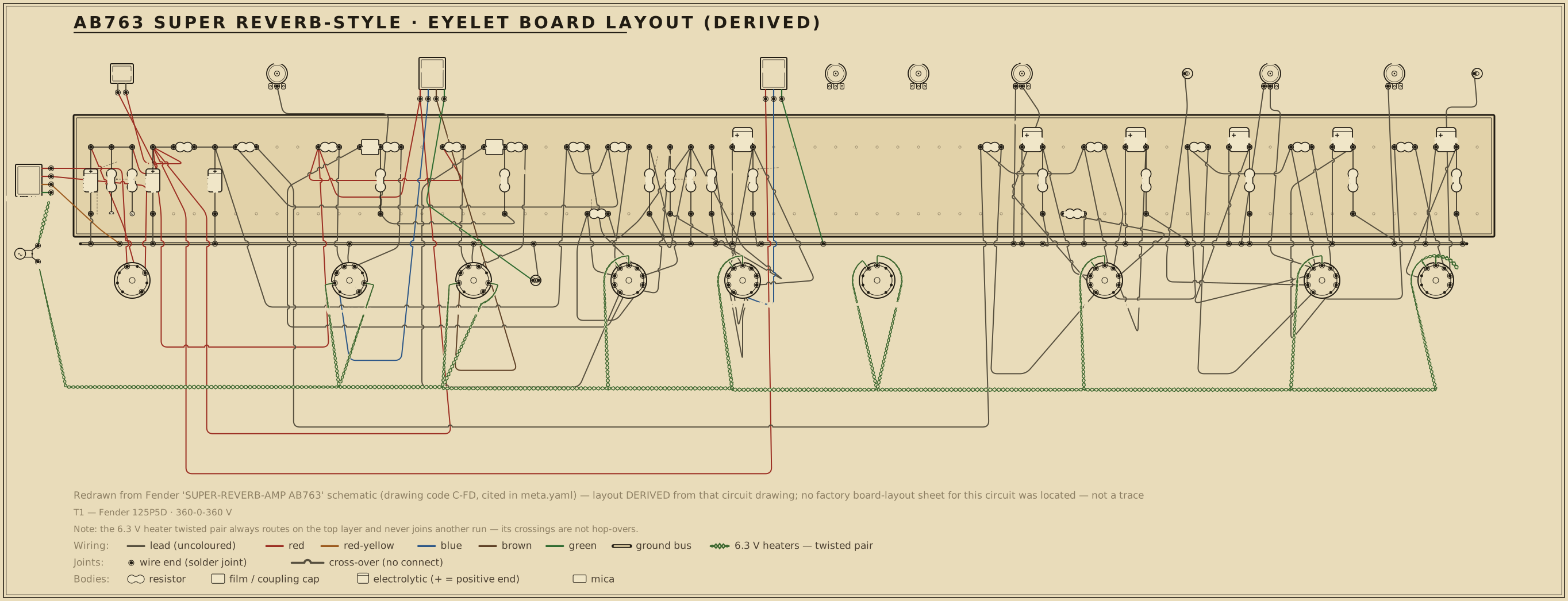
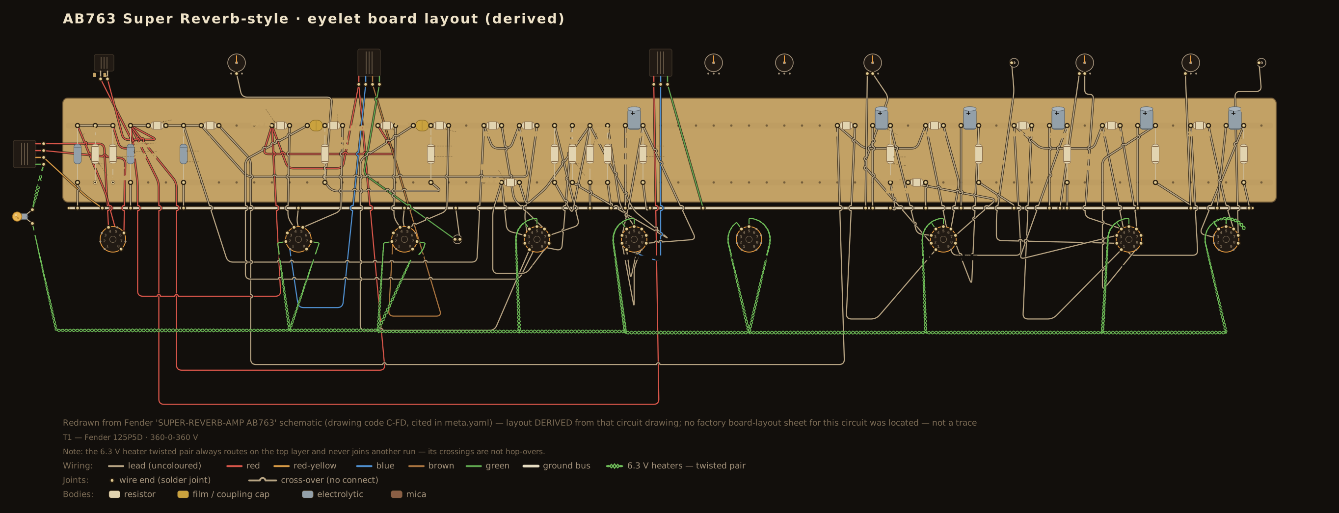
The full artifact set is present: schematic, board layout in both styles, the
social card, and the family-tier entry. The board layout is redrawn from
Fender's own layout sheet for this circuit: its parts stand in the order that
sheet mounts them, above the valve sockets in the sheet's order, with the
controls in the sheet's order above.