AB763 Blackface Deluxe Reverb-style · 1963–1967 · 22 W

✓ verified 2026-07-19
Schematic — redrawn in KiCad · scroll to zoom, drag to pan
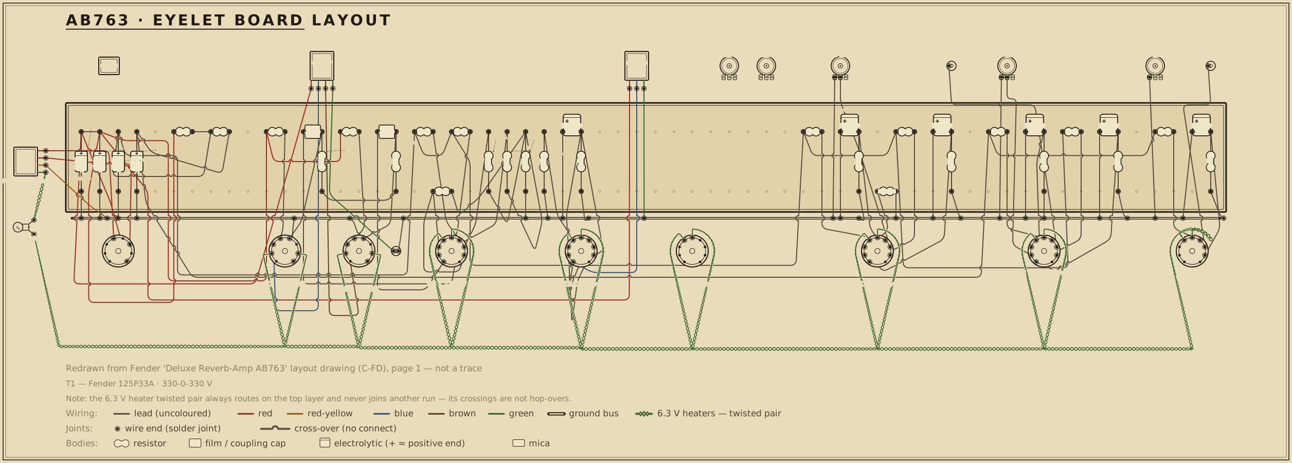
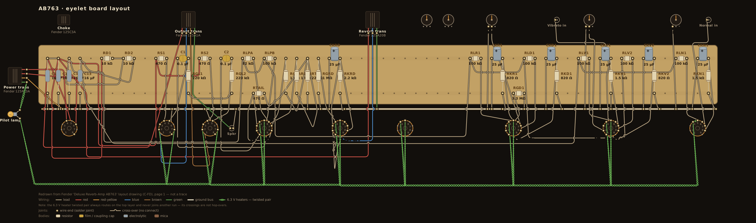
Board layout — redrawn reference diagram · source noted on the drawing
AB763 eyelet board layout — an original diagram redrawn from the published layout drawing, showing the principal parts in the order that drawing places them on the board.

Machine-checked wiring. Every modelled part the operating-point netlist places on this board — the tube sockets, the plate, cathode and grid-leak resistors, the power-rail droppers, and the coupling and bypass capacitors whose two leads are both named DC nodes — has been verified in CI, terminal for terminal, to be electrically equivalent to the simulated netlist this circuit is verified against: the same net structure, no missing or extra connections. Parts outside that DC model — the volume / tone / mixer control-network internals, the negative-bias front end, and the heater chain, pilot lamp and power-transformer / rectifier AC side — are drawn from the cited sources but are not machine-checked; the CI report enumerates every one of their terminals so the boundary is explicit rather than silent. This diagram documents connectivity and part arrangement — it is not a dimensioned 1:1 build template. Board and part positions are drawn at diagram scale, and lead dress, grounding paths, and physical spacing all matter in a high-voltage chassis. If you build from it, verify every connection against the schematic above and the operating-point table below as you go.

Operating point vs. published chart

Chart values read from the published drawing — or, where the drawing carries no voltage chart, from the cited published measurements (never reproduced). Tolerances are this project's verification targets — tighter on power rails than the ±20% measurement convention Fender printed on its charts. Simulation matches every node within target — worst deviation 10.5%.

NodeChartToleranceNote
S61 415 V ±8% 6V6 (V7) screen after its 470 Ohm-1W stopper, off the +415 plate rail
G61 -35 V ±8% 6V6 (V7) grid, fixed bias via 220k from the -35 V supply
PRD 410 V ±20% reverb-driver 12AT7 plate (paralleled sections), off BP1 through the TR4 primary DCR
KRD 8.7 V ±20% reverb-driver 12AT7 shared cathode over 2.2k
PV2 170 V ±20% vibrato-channel 2nd stage plate, 100k from +325
KV2 1.3 V ±20% vibrato-channel 2nd stage cathode over 820 Ohm
PR1 170 V ±20% reverb-recovery plate, 100k from +325
KR1 1.3 V ±20% reverb-recovery cathode over 820 Ohm
PD1 180 V ±20% vibrato/reverb mix-driver plate, 100k from +325
KD1 1.3 V ±20% mix-driver cathode over 820 Ohm
PPIA 170 V ±20% PI plate, 82k (hot) side
PPIB 180 V ±20% PI plate, 100k (cold) side
KPI 77 V ±20% PI joined cathodes, above the 470 Ohm
JPI 75.5 V ±20% PI tail junction (470 Ohm / 22k), grid-leak return
PN1 normal-channel input plate — printed +180 V. Reported, not gated: this stage's rail is shared with the excluded tremolo oscillator, so the un-loaded derived rail runs the plate high (sim ~199 V)
KN1 normal-channel input cathode over 1.5k — printed +1.3 V (informational, same shared-rail reason)
PV1 vibrato-channel input plate — printed +170 V (informational, shared-rail with the excluded tremolo)
KV1 vibrato-channel input cathode over 1.5k — printed +1.3 V (informational)

Tube-pin nodes are checked against the chart's own printed ±20% convention; power-rail nodes are held to tighter internal verification targets.

Parts list

Reference designators match the schematic above. The drawing shows one jack per channel input pair; the chassis carries two per channel. Tremolo-oscillator and reverb-tank interconnect parts are listed but the oscillator's DC point is excluded from the netlist (see notes.md).

RefPartValue / ratingRole
R1n Carbon comp resistor 68 kΩ · ½ W Normal input grid stopper (jack 1)
R2n Carbon comp resistor 68 kΩ · ½ W Normal input grid stopper (jack 2)
RGN1 Carbon comp resistor 1 MΩ · ½ W Normal input grid leak
RLN1 Carbon comp resistor 100 kΩ · ½ W V1a plate load
RKN1 Carbon comp resistor 1.5 kΩ · ½ W V1a cathode bias
CKN1 Electrolytic capacitor 25 µF · 25 V V1a cathode bypass
CTN Mica capacitor 250 pF Normal treble cap
VRTN Potentiometer 250 kΩ-A Normal treble
RSN Carbon comp resistor 100 kΩ · ½ W Normal tone-stack slope resistor
CBN Coupling capacitor 0.1 µF Normal tone-stack coupling
VRBN Potentiometer 250 kΩ-A Normal bass
CBN2 Coupling capacitor 0.047 µF Normal bass cap
RSLN Carbon comp resistor 6.8 kΩ · ½ W Normal tone-stack bleed resistor
VRVN Audio-taper potentiometer 1 MΩ-A Normal volume
R1v Carbon comp resistor 68 kΩ · ½ W Vibrato input grid stopper (jack 1)
R2v Carbon comp resistor 68 kΩ · ½ W Vibrato input grid stopper (jack 2)
RGV1 Carbon comp resistor 1 MΩ · ½ W Vibrato input grid leak
RLV1 Carbon comp resistor 100 kΩ · ½ W V2a plate load
RKV1 Carbon comp resistor 1.5 kΩ · ½ W V2a cathode bias
CKV1 Electrolytic capacitor 25 µF · 25 V V2a cathode bypass
CTV Mica capacitor 250 pF Vibrato treble cap
CBRV Mica capacitor 47 pF Vibrato bright cap
VRTV Potentiometer 250 kΩ-A Vibrato treble
VRBV Potentiometer 250 kΩ-A Vibrato bass
RSLV Carbon comp resistor 6.8 kΩ · ½ W Vibrato tone-stack bleed resistor
VRVV Audio-taper potentiometer 1 MΩ-A Vibrato volume
RLV2 Carbon comp resistor 100 kΩ · ½ W V2b (vibrato 2nd stage) plate load
RKV2 Carbon comp resistor 820 Ω · ½ W V2b cathode bias
CKV2 Electrolytic capacitor 25 µF · 25 V V2b cathode bypass
CCV2 Coupling capacitor 0.02 µF V2b output coupling
CRS Coupling capacitor 500 pF Reverb send coupling to driver grid
RGRD Carbon comp resistor 1 MΩ · ½ W Reverb-driver 12AT7 grid leak
RKRD Carbon comp resistor 2.2 kΩ · ½ W Reverb-driver shared cathode bias
CKRD Electrolytic capacitor 25 µF · 25 V Reverb-driver cathode bypass
T4 Reverb transformer Fender 125A20B Reverb driver → tank input
RGR1 Carbon comp resistor 220 kΩ · ½ W Reverb-recovery grid resistor (tank output)
RLR1 Carbon comp resistor 100 kΩ · ½ W V3b (reverb recovery) plate load
RKR1 Carbon comp resistor 820 Ω · ½ W V3b cathode bias
CKR1 Electrolytic capacitor 25 µF · 25 V V3b cathode bypass
CCR1 Coupling capacitor 0.003 µF Reverb-recovery output coupling
VRREV Linear potentiometer 100 kΩ-L Reverb level
RMR Carbon comp resistor 470 kΩ · ½ W Reverb mix resistor
RLD1 Carbon comp resistor 100 kΩ · ½ W V3a (mix driver) plate load
RGD1 Carbon comp resistor 3.3 MΩ · ½ W V3a grid leak (tremolo shunt node)
RKD1 Carbon comp resistor 820 Ω · ½ W V3a cathode bias
CKD1 Electrolytic capacitor 25 µF · 25 V V3a cathode bypass
CBD1 Mica capacitor 10 pF V3a grid bright cap
RMD1 Carbon comp resistor 220 kΩ · ½ W Mix-driver to PI grid resistor
CCD1 Coupling capacitor 0.001 µF Mix-driver → PI coupling
VRSPD Reverse-audio potentiometer 3 MΩ-RA Tremolo speed
VRINT Reverse-audio potentiometer 50 kΩ-RA Tremolo intensity
RTO1 Carbon comp resistor 100 kΩ · ½ W Tremolo oscillator plate load
RTO2 Carbon comp resistor 220 kΩ · ½ W Tremolo oscillator plate load
RTOG Carbon comp resistor 2.2 MΩ · ½ W Tremolo oscillator grid
RTOG2 Carbon comp resistor 1 MΩ · ½ W Tremolo phase-shift resistor
RTOG3 Carbon comp resistor 1 MΩ · ½ W Tremolo phase-shift resistor
RTO10 Carbon comp resistor 10 MΩ · ½ W Tremolo oscillator grid leak
RKTO1 Carbon comp resistor 2.7 kΩ · ½ W Tremolo oscillator cathode
RKTO2 Carbon comp resistor 100 kΩ · ½ W Tremolo oscillator cathode/plate
CTO1 Film capacitor 0.01 µF Tremolo phase-shift cap
CTO2 Film capacitor 0.01 µF Tremolo phase-shift cap
CTO3 Film capacitor 0.02 µF Tremolo phase-shift cap
RINT Carbon comp resistor 10 kΩ · ½ W Tremolo intensity series
OPTO Optocoupler neon lamp + photoresistor Tremolo modulator (shunts V3a grid)
RLPA Carbon comp resistor 82 kΩ · ½ W · 5% PI plate load (hot side)
RLPB Carbon comp resistor 100 kΩ · ½ W · 5% PI plate load (cold side)
RGPA Carbon comp resistor 1 MΩ · ½ W PI grid leak (hot), returned to tail junction
RGPB Carbon comp resistor 1 MΩ · ½ W PI grid leak (cold), returned to tail junction
RTAIL Carbon comp resistor 470 Ω · ½ W PI cathode resistor
RT2 Carbon comp resistor 22 kΩ · ½ W PI tail (junction → ground)
CPIA Coupling capacitor 0.001 µF PI hot-grid input coupling
CPIB Coupling capacitor 0.1 µF · 200 V PI cold-grid AC ground
RNFB Carbon comp resistor 820 Ω · ½ W Negative feedback, OT secondary → PI (DC-neutral)
RNF2 Carbon comp resistor 47 Ω · ½ W NFB return / PI cold-grid reference
C1 Coupling capacitor 0.1 µF · 400 V PI hot plate → V7 grid
C2 Coupling capacitor 0.1 µF · 400 V PI cold plate → V8 grid
RGL1 Carbon comp resistor 220 kΩ · ½ W · 5% V7 grid leak, from the −35 V bias line
RGL2 Carbon comp resistor 220 kΩ · ½ W · 5% V8 grid leak, from the −35 V bias line
RS1 Wirewound resistor 470 Ω · 1 W V7 screen resistor
RS2 Wirewound resistor 470 Ω · 1 W V8 screen resistor
T3 Output transformer Fender 125A1A Push-pull 6V6 output
T1 Power transformer Fender 125P33A · 330-0-330 V HT + heaters + rectifier filament
T2 Filter choke Fender 125C3A Reservoir → screen rail
C10 Electrolytic capacitor 16 µF · 450 V (×2) Reservoir filter (post-standby)
C11 Electrolytic capacitor 16 µF · 450 V Filter, node B (screens/+415)
C12 Electrolytic capacitor 16 µF · 450 V Filter, node C (+325 PI/preamp)
C13 Electrolytic capacitor 16 µF · 450 V Filter, node D (input-stage rail)
RD1 Carbon comp resistor 10 kΩ · ½ W Rail dropper B → C
RD2 Carbon comp resistor 10 kΩ · ½ W Rail dropper C → D
RBIAS Wirewound resistor 470 Ω · 1 W Bias-supply series resistor
DBIAS Rectifier (bias) silicon diode Bias-supply rectifier
CB1 Electrolytic capacitor 25 µF · 50 V Bias-supply filter
CB2 Electrolytic capacitor 50 µF · 50 V Bias-supply filter
VRBAL Linear potentiometer 10 kΩ-L Hum-balance / bias divider
RBAL Carbon comp resistor 10 kΩ · ½ W Bias divider
CDEATH Ceramic capacitor 0.047 µF · 600 V Ground-switch cap (period; not in modern builds)
V1 Preamp tube 12AX7 (7025) Normal channel input (V1a)
V2 Preamp tube 12AX7 (7025) Vibrato channel input + 2nd stage (V2a/V2b)
V3 Preamp tube 12AX7 (7025) Reverb recovery + mix driver (V3a/V3b)
V4 Preamp/driver tube 12AT7 Reverb driver (both sections paralleled)
V5 Preamp tube 12AX7 Tremolo oscillator (DC point excluded)
V6 Preamp/driver tube 12AT7 Long-tailed-pair phase inverter
V7 Power tube 6V6GT Push-pull output (hot side)
V8 Power tube 6V6GT Push-pull output (cold side)
V9 Rectifier tube GZ34 Full-wave rectifier (V9A/V9B)

Circuit story

The circuit most players picture when they think "Fender clean": a 22-watt, 6V6 combo with tube reverb and a genuine tremolo, built on the AB763 chassis that ran from 1963 to 1967. Two channels share the output stage — a plain Normal channel and a Vibrato channel carrying the reverb and the tremolo — feeding a fixed-biased 6V6GT pair through a 12AT7 phase inverter, rectified by a GZ34. The preamp bottles are marked 7025 on the drawing, the low-noise selected version of the 12AX7; the reverb driver and phase inverter are 12AT7s, chosen for the current they can deliver.

Signal path

Normal channel. Two inputs (each a 68 kΩ stopper on a 1 MΩ leak) → first 12AX7 stage (100 kΩ plate load, 1.5 kΩ cathode with a 25 µF bypass) → a treble-bass tone stack (250 kΩ treble and bass, 6.8 kΩ bleed, 250 pF and 0.047 µF caps) and a 1 MΩ volume → the mixing resistor into the phase inverter. No reverb, no tremolo.

Vibrato channel. Input stage as above → tone stack (with a 47 pF bright cap across the treble) and volume → a second 12AX7 stage (100 kΩ plate, 820 Ω cathode) → the reverb and tremolo section.

Reverb. The dry vibrato signal drives a 12AT7 with both triodes in parallel (2.2 kΩ shared cathode) into the 125A20B transformer and the spring tank. The returned signal comes back through a 12AX7 recovery stage (100 kΩ plate, 820 Ω cathode) and is blended back with the dry signal by the 100 kΩ Reverb control, then handed to the mix driver that feeds the inverter.

Tremolo. A 12AX7 phase-shift oscillator (Speed on a 3 MΩ control) drives an optocoupler — a neon lamp facing a photoresistor — that periodically shunts the mix-driver's grid to ground, swinging the volume up and down. The Intensity control sets how hard the lamp is driven.

Phase inverter and output. A 12AT7 long-tailed pair (82 kΩ and 100 kΩ 5% plate loads, a 470 Ω cathode resistor to a tail junction, 22 kΩ tail to ground, both 1 MΩ grid leaks returned to that junction) splits the signal for the 6V6GT pair. The output tubes are fixed-biased at −35 V through 220 kΩ leaks, with 470 Ω · 1 W screen resistors, and an 820 Ω negative-feedback loop returns from the speaker to the inverter.

Power

330-0-330 V (power transformer 125P33A) → GZ34+415 V at the 6V6 plates (the output transformer centre tap sits at +420 V) → filter choke → +415 V screens → a 10 kΩ dropper → +325 V at the phase-inverter plates and the 820 Ω-cathode preamp stages → a second 10 kΩ dropper → the channel-input rail. A separate negative supply — a 470 Ω · 1 W feed, a rectifier, 25 µF and 50 µF cans and a 10 kΩ divider — provides the −35 V fixed bias.

Bias and lineage

Where the tweed Deluxe cathode-biased its 6V6s, the blackface Deluxe Reverb runs a proper negative-bias supply — the recipe it inherited from the brownface Deluxe (the 6G3) rather than from any tweed. That ancestry edge lands in the lineage graph when the 6G3 does.

Reading against the printed chart

The drawing prints a full voltage chart, every value set at ±20 %, read to ground with an electronic voltmeter. The simulated DC operating point tracks it across the modelled stages: the reverb-driver plate lands at +414 V against a printed +410 V, the phase-inverter plates and the +77 V / +75.5 V tail fall within a tenth of the chart, and the 6V6 screens sit at +415 V with their grids on the −35 V bias line. Two nodes are reported for information only:

  • The two channel-input plates. Their supply rail is shared with the tremolo oscillator, a phase-shift oscillator that has no static operating point and so is left out of the DC solution. With that load absent, the rail runs above its loaded factory value and the two input plates read high — so the printed +180 V / +170 V are shown for reference rather than compared.

  • The tremolo oscillator. Its printed pins (+270 V plate, +2.1 V cathode) are the running average a meter reads while it swings, set by grid-leak detection. Solved as a quiescent stage, the 220 kΩ / 2.7 kΩ node sits near +200 V — about a quarter below the printed +270 V — so it is reported rather than fitted to the chart.

Every gated node verifies against the printed chart within the drawing's own ±20 % convention — the worst sits about a tenth off — with the tremolo oscillator and the two shared-rail input plates set aside above as documented exclusions rather than force-fitted to the chart.

Sources