5F4 Tweed Super‑style · 1957–1960 · 26 W

✓ verified 2026-08-03
Schematic — redrawn in KiCad · scroll to zoom, drag to pan
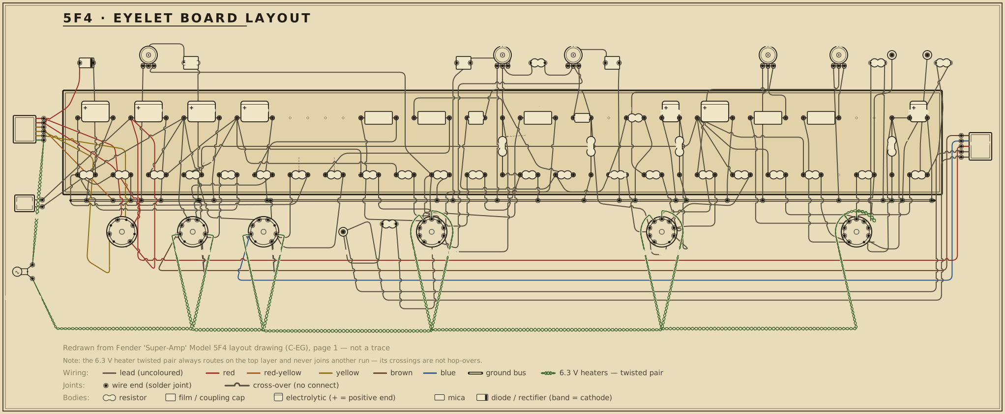
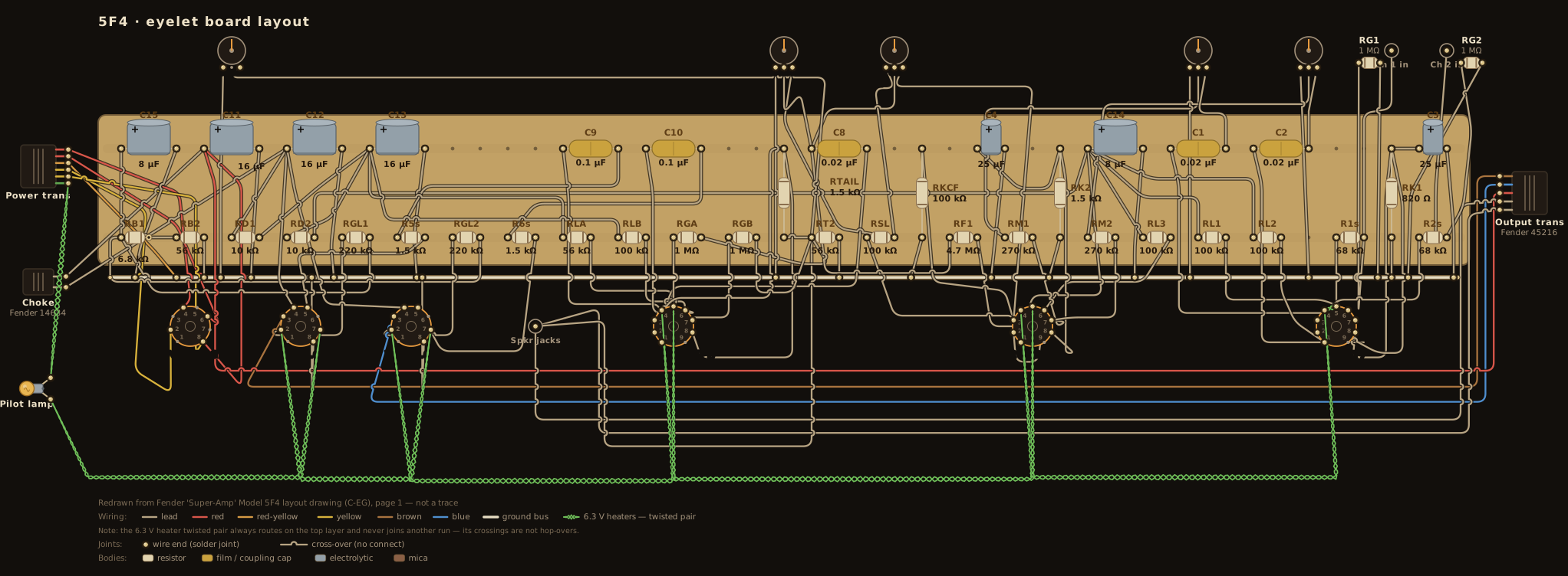
Board layout — redrawn reference diagram · source noted on the drawing Print sheet ↗
5F4 eyelet board layout — an original diagram redrawn from the published layout drawing, showing the principal parts in the order that drawing places them on the board, drawn in the period layout-sheet style with each value lettered on the part.

Scroll the drawing sideways to read the whole board — the source line and the colour legend run along the bottom of the sheet — or open the full-size diagram in its own tab. Values are lettered on the parts in the period shorthand — .02-400, 250-5, 1MEG: how to read it.

Machine-checked wiring. Every modelled part the operating-point netlist places on this board has been verified in CI, terminal for terminal, to be electrically equivalent to the simulated netlist this circuit is verified against. This diagram documents connectivity and part arrangement — it is not a dimensioned 1:1 build template.

Details

The modelled parts are the tube sockets, the plate, cathode and grid-leak resistors, the power-rail droppers, and the coupling and bypass capacitors whose two leads are both named DC nodes; the check proves the same net structure, with no missing or extra connections. Parts outside that DC model — the volume / tone / mixer control-network internals, the negative-bias front end, and the heater chain, pilot lamp and power-transformer / rectifier AC side — are drawn from the cited sources but are not machine-checked; the CI report enumerates every one of their terminals so the boundary is explicit rather than silent.

Board and part positions are drawn at diagram scale, and lead dress, grounding paths, and physical spacing all matter in a high-voltage chassis. If you build from it, verify every connection against the schematic above and the operating-point table below as you go.

Operating point vs. published chart

Chart values read from the published drawing — or, where the drawing carries no voltage chart, from the cited published measurements (never reproduced). The simulated column is this circuit's own netlist solved in ngspice by the run that gates it; every deviation beside it is those two numbers compared, not a separately stated figure. Tolerances are this project's verification targets: tube-pin nodes carry the tolerance the cited source states, or ±20% — the era's printed convention — where it states none, and power rails are held to tighter internal targets. Every gated node lands within target — worst deviation 16%.

Node Chart Simulated Deviation Tolerance Note
BP2 410 V 413.3 V 0.8% ±8% screens node after the choke (DCR estimated at 130 Ω)
BP3 332 V 335.6 V 1.1% ±8% PI supply node after the first 10 kΩ dropper
BP4 280 V 280.4 V 0.1% ±8% preamp node after the second 10 kΩ dropper
PAY1 140 V 144.4 V 3.1% ±20% 12AY7 plate (channel 1)
PAY2 140 V 144.4 V 3.1% ±20% 12AY7 plate (channel 2)
KAY 2.2 V 2.2 V 1.4% ±20% shared 12AY7 cathode, 820 Ω
P2A
chart disputed
140 V 183.2 V 30.9% not gated
The printed pair (140 V plate, 2.2 V cathode) is physically impossible for a 12AX7 …

2.2 V across 1.5 kΩ implies 1.47 mA, which at Vg ≈ −2.2 V requires roughly 280 V plate-to-cathode — twice the printed value. Philips' measured resistance-coupled tables and simulation both put the self-consistent point near 190 V.

K2A
chart disputed
2.2 V 1.5 V 33.8% not gated Half of the physically-impossible printed pair on V2A — see P2A.
KCF
chart disputed
140 V 182.9 V 30.7% not gated
Direct-coupled to V2A's plate, so it inherits the disputed printed 140 V …

simulation follows the self-consistent operating point near 190 V.

PPIA 213 V 220.9 V 3.7% ±20% V3A (driver) plate, 100 kΩ load — consistent with the printed +1.7 V cathode: ≈1.2 mA through both
KPIA 1.7 V 1.7 V 1.2% ±20% V3A cathode, 1.5 kΩ (printed beside the tube; the NFB/presence network landing here is DC-neutral to within a few percent)
PPIB 270 V 273.7 V 1.4% ±20% V3B (cathodyne) plate, 56 kΩ load
KPI 55 V 63.5 V 15.5% ±20% V3B cathode, 1.5 kΩ above the 56 kΩ leg — the printed 55/53.3 pair implies the same ≈1 mA the plate figure does
JPI 53.3 V 61.8 V 16.0% ±20% 1.5 kΩ/56 kΩ junction — the cathodyne grid's DC reference through the 1 MΩ leak
G51 −40 V −40.0 V 0.0% ±8% 6L6G fixed bias via 220k from the -40 V supply

Tube-pin nodes are checked at the tolerance the cited source states, or at the era's ±20% convention where it states none; power-rail nodes are held to tighter internal verification targets. A node marked chart disputed is excluded from that check — its printed value contradicts the rest of the chart, and the note says how; its deviation is shown for the record, not as a result. Simulated figures are the netlist's DC solution, not measurements from a chassis.

The output stage behind these numbers can be drawn: the load line explorer plots this circuit's 6L6G pair at the DC operating point its netlist carries — 415 V on the plates with a −40 V grid bias — and marks where the load line crosses.

Parts list

Every designator in this list appears on the schematic above, and every designator on the schematic appears here — the two are checked against each other in both directions, a valve's two halves counting as one bottle (V1A and V1B are both V1). Three parts the drawing carries as annotations rather than numbered symbols are listed here without designators, and stand outside that check. The schematic draws one jack per channel (the chassis has four). Output tubes are drawn '6L6G' on the C-EG sheet; Fender shipped the tweed Super with 5881s (interchangeable 6L6-family) and the 5881 SPICE model stands in for simulation. The tone network is capacitor-isolated and omitted from the DC netlist (the phase-inverter grid's DC path through it is modelled as a single leak resistor). The negative-feedback resistor, the presence pot and its 0.1 µF bleed cap are chassis wiring rather than board wiring, but the drawing carries all three, so they carry designators (RNF, VR6, C17) and are drawn on the schematic. Parts drawn only as annotations (bright cap, line caps, power transformer) are listed without designators.

RefPartValue / ratingRole
R1s Carbon comp resistor 68 kΩ · ½ W Channel-1 grid stopper
R2s Carbon comp resistor 68 kΩ · ½ W Channel-2 grid stopper
RG1 Carbon comp resistor 1 MΩ · ½ W Channel-1 input grid leak
RG2 Carbon comp resistor 1 MΩ · ½ W Channel-2 input grid leak
RL1 Carbon comp resistor 100 kΩ · ½ W V1A plate load
RL2 Carbon comp resistor 100 kΩ · ½ W V1B plate load
RK1 Carbon comp resistor 820 Ω · ½ W Shared 12AY7 cathode bias
C3 Electrolytic capacitor 25 µF · 25 V Shared 12AY7 cathode bypass
C1 Coupling capacitor 0.02 µF · 600 V V1A → channel-1 volume
C2 Coupling capacitor 0.02 µF · 600 V V1B → channel-2 volume
VR1 Audio-taper potentiometer 1 MΩ Channel-1 volume (100 pF bright cap across it)
VR2 Audio-taper potentiometer 1 MΩ Channel-2 volume
RM1 Carbon comp resistor 270 kΩ · ½ W Channel-1 mixer
RM2 Carbon comp resistor 270 kΩ · ½ W Channel-2 mixer
RL3 Carbon comp resistor 100 kΩ · ½ W V2A plate load
RK2 Carbon comp resistor 1.5 kΩ · ½ W V2A cathode bias
C4 Electrolytic capacitor 25 µF · 25 V V2A cathode bypass
RKCF Carbon comp resistor 100 kΩ · ½ W Cathode-follower load
RF1 Carbon comp resistor 4.7 MΩ · ½ W V2A grid reference / feedback, returned to the tone network's bass-branch node
RSL Carbon comp resistor 100 kΩ · ½ W Tone network — bass-branch series resistor, coupler node → the bass pot's wiper
C5 Mica capacitor 250 pF Tone network — treble capacitor
VR3 Potentiometer (taper not marked on the drawing) 1 MΩ Treble
C6 Film capacitor 0.01 µF · 600 V Tone network — treble-pot cold end to ground
C7 Film capacitor 0.005 µF · 600 V Tone network — bass-pot leg capacitor to ground
C16 Film capacitor 0.1 µF · 200 V Tone network — bass-branch coupling capacitor
RSH Carbon comp resistor 220 kΩ · ½ W Tone network — bass-branch leak to ground
RSR Carbon comp resistor 220 kΩ · ½ W Tone network — bass branch into the stack output (the phase-inverter grid)
VR4 Audio-taper potentiometer 1 MΩ Bass (the network injects at its wiper)
RLA Carbon comp resistor 100 kΩ · ½ W V3A (driver) plate load
RK3 Carbon comp resistor 1.5 kΩ · ½ W V3A cathode bias (the 56 kΩ NFB and the presence network land here)
C8 Coupling capacitor 0.02 µF · 600 V Driver plate → cathodyne grid
RGB Carbon comp resistor 1 MΩ · ½ W Cathodyne grid leak, returned to the 1.5 kΩ/56 kΩ cathode junction
RLB Carbon comp resistor 56 kΩ · ½ W V3B (cathodyne) plate load
RKA Carbon comp resistor 1.5 kΩ · ½ W Cathodyne cathode resistor (cathode → the 56 kΩ junction)
RKB Carbon comp resistor 56 kΩ · ½ W Cathodyne cathode load (junction → ground)
RNF Carbon comp resistor 56 kΩ · ½ W Negative feedback, speaker → V3A (driver) cathode
VR6 Linear potentiometer 5 kΩ Presence — from the driver's cathode to ground
C17 Film capacitor 0.1 µF · 200 V Presence wiper to ground
C9 Coupling capacitor 0.1 µF · 400 V Cathodyne plate → V4 grid
C10 Coupling capacitor 0.1 µF · 200 V Cathodyne cathode → V5 grid
R5s Carbon comp resistor 1.5 kΩ · ½ W V4 grid stopper
R6s Carbon comp resistor 1.5 kΩ · ½ W V5 grid stopper
RGL1 Carbon comp resistor 220 kΩ · ½ W V4 grid leak, from the −40 V bias line
RGL2 Carbon comp resistor 220 kΩ · ½ W V5 grid leak, from the −40 V bias line
RD1 Power resistor 10 kΩ Rail dropper B+2 → B+3
RD2 Power resistor 10 kΩ Rail dropper B+3 → B+4
L1 Filter choke Fender 14684 B+1 → B+2 (screens)
C11 Electrolytic capacitor 16 µF · 450 V Filter, B+1 (reservoir)
C12 Electrolytic capacitor 16 µF · 450 V Filter, B+2
C13 Electrolytic capacitor 16 µF · 450 V Filter, B+3
C14 Electrolytic capacitor 8 µF · 450 V Filter, B+4
D1 Rectifier (bias) selenium (silicon diode in modern builds) Bias supply rectifier
RB1 Carbon comp resistor 6.8 kΩ · ½ W Bias supply series resistor
RB2 Carbon comp resistor 56 kΩ · ½ W Bias supply bleeder
C15 Electrolytic capacitor 8 µF · 150 V Bias supply filter
V1 Preamp tube 12AY7 Both input stages (V1A/V1B)
V2 Preamp tube 12AX7 Gain stage + cathode follower (V2A/V2B)
V3 Preamp tube 12AX7 Phase-inverter driver + split-load cathodyne (V3A/V3B)
V4 Power tube 6L6G Push-pull output (upper)
V5 Power tube 6L6G Push-pull output (lower)
V6 Rectifier tube 5U4G Full-wave rectifier (V6A/V6B)
T3 Output transformer Fender 45216 Push-pull output into 2 × 10 in speakers
Power transformer Fender 8087 HT + heaters + rectifier filament
Mica capacitor 100 pF Bright cap across VR1 (annotation only on schematic)
Film capacitor 0.05 µF · 600 V (×2) AC-line filter caps (annotation only)

Circuit story

The tweed Super shares the Bassman's front half — a 12AY7 two-channel front end, a 12AX7 gain stage feeding a direct-coupled cathode follower, and a fixed-bias pair of 6L6-family output tubes — but its back half is its own circuit: a split treble/bass tone network unlike the Bassman ladder, and a driver + split-load (cathodyne) phase inverter rather than a long-tailed pair. Produced across the late-tweed years (1957–1960), it shares the 5F6-A's power iron almost part-for-part (PT 8087, choke 14684, a 5881/6L6G pair biased near −40 V) while running a slightly lower rail set. Its direct ancestor is the narrow-panel 5E4-A, which it follows stage for stage — the same two-channel 12AY7 front end, the same cathode-follower treble/bass network, the same driver + split-load cathodyne, the same selenium bias supply — changing the output pair back to 6L6G and lifting the rails.

Circuit walkthrough (short form)

Two channels (each: 1M grid leak, 68k stopper) → V1 12AY7 (100k plates, shared 820 Ω cathode with 25 µF bypass) → 0.02 µF couplers → 1M volume pots → 270k mixers → V2A 12AX7 (100k plate, 1.5k/25 µF cathode) → V2B cathode follower, DC-coupled (100k cathode load) → the split tone network (below) → straight into the grid of V3A, a cathode-biased 12AX7 driver stage (100k plate, 1.5k cathode) → 0.02 µF → V3B split-load cathodyne: 56k plate, 1.5k

  • 56k under the cathode, 1M grid leak returned to the 1.5k/56k junction → 0.1 µF couplers from the cathodyne's plate and cathode6L6G pair, fixed-biased at −40 V through 220k leaks (1.5k grid stoppers), screens tied straight to the +410 V node → Fender 45216 output transformer into the two 10-inch speakers. A 56k negative-feedback resistor returns from the speaker to V3A's cathode, where the 5k presence pot bleeds it to ground through 0.1 µF.

Power: 5U4G rectifier → +415 V reservoir (output plates) → choke (14684) → +410 V screens → 10k → +332 V phase-inverter supply → 10k → +280 V preamp. A selenium rectifier with a 6.8k/56k network supplies the −40 V bias.

The output tubes are lettered 6L6G on the C-EG sheet; Fender equipped the tweed Super with 5881s, the ruggedized 6L6 the Bassman and Twin also used, and the two are interchangeable. Simulation here uses the 6L6-family 5881 model.

The tone network the sheet draws

The 5F4's two knobs are not a two-knob cut of the Bassman stack — the C-EG sheet draws a different network, in which treble and bass ride two separate branches off the cathode follower and recombine at the phase inverter's grid:

  • Treble: the follower's cathode feeds a 250 pF capacitor into one end of the 1M treble pot; the pot's other end reaches ground through 0.01 µF, and the wiper is the output.
  • Bass: the cathode also feeds a 0.1 µF coupler into a node carrying a 220k leak to ground (the amp's 4.7M feedback resistor returns here too), then 100k in series into the 1M bass pot's wiper — the branch injects at the wiper, not at an end lug. One end lug reaches ground through 0.005 µF, the other is grounded outright. From the wiper node, 220k carries the branch to the output.
  • The recombined output node is the driver's grid: no coupling capacitor and no grid-leak resistor follow the network — its own 220k-and-track path to ground sets the grid's DC.

There is no slope resistor and no shared cap ladder, so the two controls interact far less than the Bassman family's do — and the treble and bass curves cross over with no scoop carved between them.

The phase inverter the sheet draws

The C-EG drawing prints no long-tailed pair. V3A is a plain cathode-biased gain stage — 100k plate at the printed +213 V over a 1.5k cathode at +1.7 V — and V3B is a split-load cathodyne: 56k in the plate (printed +270 V), 1.5k

  • 56k under the cathode (printed +55 V and +53.3 V), with the 1M grid leak returned to the 1.5k/56k junction so the stage biases itself. The two 0.1 µF output couplers leave from the cathodyne's plate and cathode — one inverted output, one not, which is the whole job. The 56k feedback resistor and the 5k presence pot land on V3A's cathode: cathode-injected feedback, with the presence control varying how much of it the 0.1 µF bleeds to ground.

Verification — and what the chart gets wrong

The rails, the 12AY7 front end, all five phase-inverter values, and the 6L6 fixed-bias supply verify against the printed chart (worst gated node 16.0 %, against the chart's own ±20 % convention). The five phase-inverter figures — +213/+1.7 on the driver, +270/+55/+53.3 on the cathodyne — are mutually consistent once the stage is read as the driver + cathodyne the sheet draws; an earlier revision of this page modelled a long-tailed pair here and had to dispute three of them as contradictory, which they never were. Three printed values remain excluded as disputed, with the arithmetic shown in the voltage table: the chart's V2A pair (140 V plate with a 2.2 V cathode) is physically impossible for a 12AX7 — that cathode voltage implies a current the tube can only pass near 280 V — and the cathode follower inherits the same printed value through its direct coupling. Measured period data and simulation agree the real operating point sits near 190 V. The full analysis is in the archive's 12AX7 calibration study.

Sources