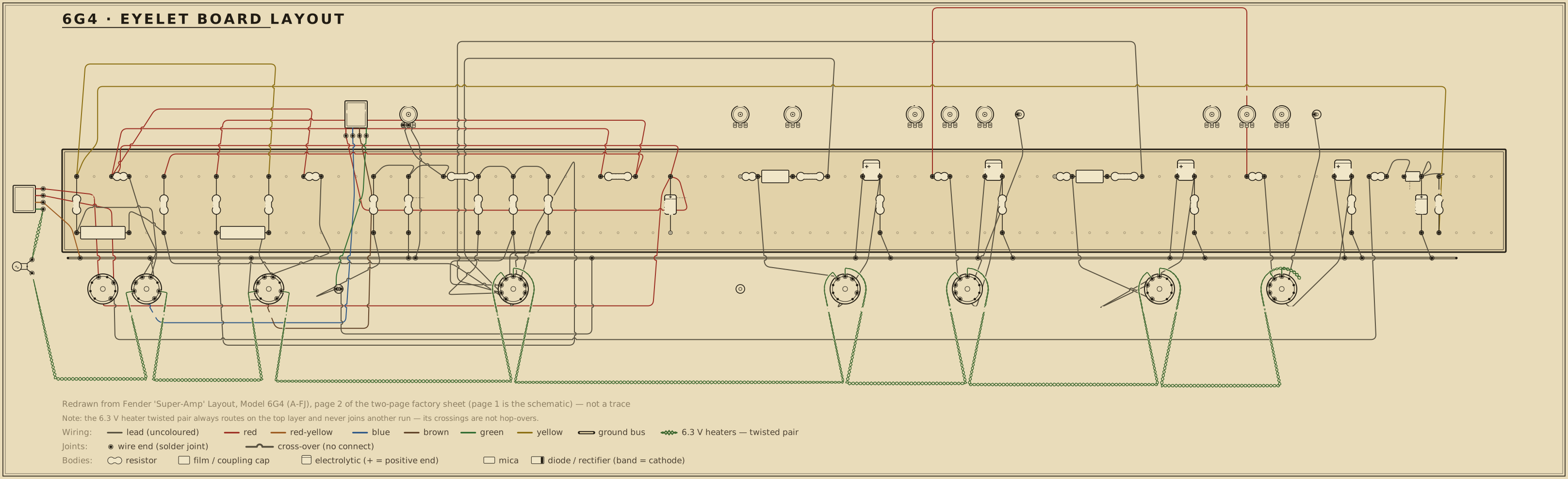
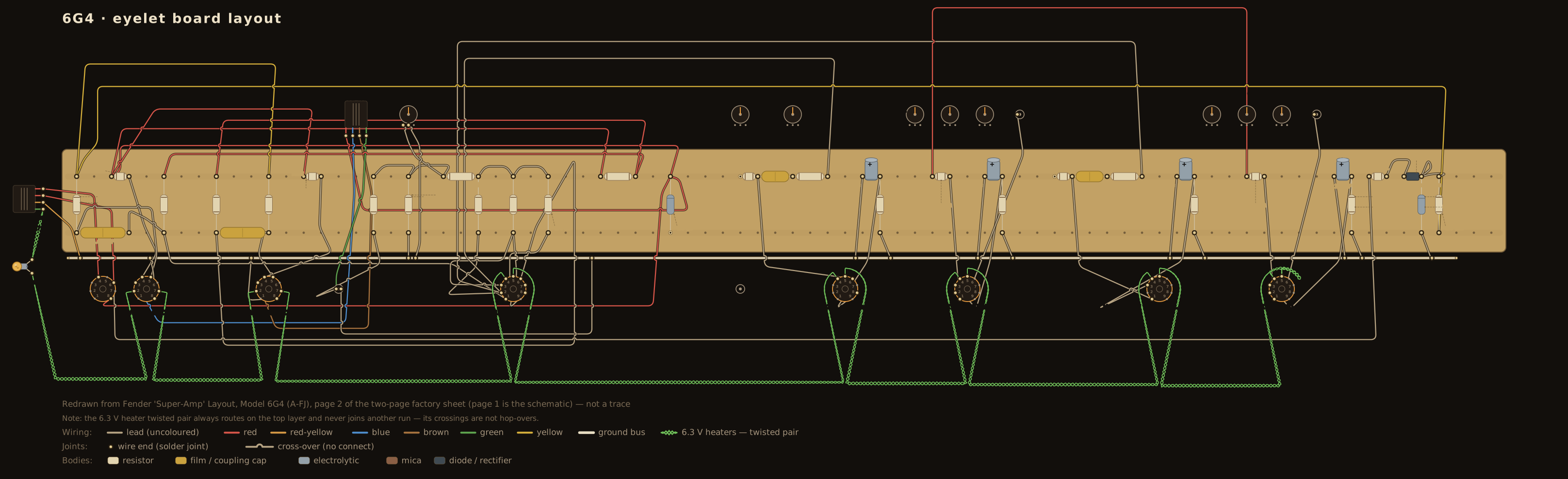
| R1a | Carbon comp resistor | 68 kΩ · ½ W | Channel-1 grid stopper from input 1 |
| R2a | Carbon comp resistor | 68 kΩ · ½ W | Channel-1 grid stopper from input 2 |
| RG1I | Carbon comp resistor | 1 MΩ · ½ W | Channel-1 leak at input 1, to ground (mounted at the jack) |
| RL1I | Carbon comp resistor | 100 kΩ · ½ W | V1A plate load, off rail A |
| CC1T | Coupling capacitor | 0.05 µF | Channel-1 first-stage plate into the tone network — the stack's coupling capacitor, lettered .05 on the drawing and mounted on the board beside the plate load |
| CT1 | Mica capacitor | 250 pF | Channel-1 treble cap (250MM on the drawing), stack input to the Treble pot's hot lug; mounts at the Treble pot |
| VRT1 | Potentiometer | 250 kΩ-L | Channel-1 treble — hot lug on the 250 pF, cold lug on the slope foot, wiper to the Volume pot |
| RS1T | Carbon comp resistor | 100 kΩ · ½ W | Channel-1 tone-stack slope resistor, stack input to the slope foot; mounts at the Treble pot |
| VRB1 | Potentiometer | 250 kΩ-A | Channel-1 bass — a divider from the slope foot to ground: the 0.01 µF across its upper section (hot lug to wiper), the 10 kΩ foot across its lower (wiper to ground) |
| CB1T | Film capacitor | 0.01 µF | Channel-1 bass capacitor, slope foot to the Bass pot's wiper; mounts at the Bass pot |
| RSL1 | Carbon comp resistor | 10 kΩ · ½ W | Channel-1 bass foot resistor, the Bass pot's wiper to ground; mounts at the Bass pot |
| VRV1 | Potentiometer | 500 kΩ-L | Channel-1 volume, fed from the Treble wiper; its own wiper is V2A's grid |
| CBR1 | Mica capacitor | 47 pF | Channel-1 bright capacitor across the Volume pot, hot lug to wiper (47MM on the drawing); mounts at the Volume pot |
| RL1D | Carbon comp resistor | 100 kΩ · ½ W | V2A plate load, from the plate to the decoupling junction |
| RLD1 | Carbon comp resistor | 6.8 kΩ · ½ W | V2A load decoupler, junction to rail A (lettered 6800); channel 1's output is taken at this junction, not at the plate |
| CC1D | Coupling capacitor | 0.05 µF | Channel-1 output, from the decoupling junction into the vibrato's band-splitting filters |
| R1b | Carbon comp resistor | 68 kΩ · ½ W | Channel-2 grid stopper from input 1 |
| R2b | Carbon comp resistor | 68 kΩ · ½ W | Channel-2 grid stopper from input 2 |
| RG2I | Carbon comp resistor | 1 MΩ · ½ W | Channel-2 leak at input 1, to ground (mounted at the jack) |
| RL2I | Carbon comp resistor | 100 kΩ · ½ W | V1B plate load, off rail A |
| CC2T | Coupling capacitor | 0.05 µF | Channel-2 first-stage plate into the tone network — as CC1T |
| CT2 | Mica capacitor | 250 pF | Channel-2 treble cap — as CT1 |
| VRT2 | Potentiometer | 250 kΩ-L | Channel-2 treble — as VRT1 |
| RS2T | Carbon comp resistor | 100 kΩ · ½ W | Channel-2 tone-stack slope resistor — as RS1T |
| VRB2 | Potentiometer | 250 kΩ-A | Channel-2 bass — a divider from the slope foot to ground, as VRB1 |
| CB2T | Film capacitor | 0.01 µF | Channel-2 bass capacitor — as CB1T |
| RSL2 | Carbon comp resistor | 10 kΩ · ½ W | Channel-2 bass foot resistor — as RSL1 |
| VRV2 | Potentiometer | 500 kΩ-L | Channel-2 volume, fed from the Treble wiper; its wiper is V2B's grid. Neither page draws a bright capacitor on this control |
| RL2D | Carbon comp resistor | 220 kΩ · ½ W | V2B plate load, off rail A — the reason this plate prints +120 V against channel 1's +160 V |
| CC2D | Coupling capacitor | 0.05 µF | Channel-2 output coupler |
| RM2 | Carbon comp resistor | 1 MΩ · ½ W | Channel-2 mixing resistor into the node where the vibrato pair's outputs recombine |
| RKI | Carbon comp resistor | 820 Ω · ½ W | V1 cathode resistor — both first stages' cathodes joined (the drawing's boxed C) |
| CKI | Electrolytic capacitor | 25 µF · 25 V | V1 cathode bypass (25-25 on the drawing) |
| RKD | Carbon comp resistor | 820 Ω · ½ W | V2 cathode resistor — both second stages' cathodes joined (the drawing's boxed D) |
| CKD | Electrolytic capacitor | 25 µF · 25 V | V2 cathode bypass (25-25 on the drawing) |
| RLP | Carbon comp resistor | 470 kΩ · ½ W | Low-band branch series resistor, channel-1 output to the low-pass node |
| CLP | Film capacitor | 0.005 µF | Low-band branch shunt, low-pass node to ground |
| CV1 | Film capacitor | 0.01 µF | Low-band coupler, low-pass node to V4A's grid |
| RHP1 | Carbon comp resistor | 220 kΩ · ½ W | High-band branch, channel-1 output to the high-pass node |
| RHP2 | Carbon comp resistor | 220 kΩ · ½ W | High-band branch, high-pass node to ground |
| CV2 | Mica capacitor | 250 pF | High-band coupler (250MM on the drawing), high-pass node to V4B's grid |
| RLV1 | Carbon comp resistor | 100 kΩ · ½ W | V4A (low band) plate load, off the +350 V vibrato-pair supply |
| RLV2 | Carbon comp resistor | 100 kΩ · ½ W | V4B (high band) plate load, off the +350 V vibrato-pair supply |
| RKV | Carbon comp resistor | 4.7 kΩ · ½ W | Vibrato pair's joined cathodes to ground |
| CKV | Electrolytic capacitor | 2 µF · 25 V | Vibrato pair's cathode bypass (lettered 2-25 on both pages) |
| RGV1 | Carbon comp resistor | 1 MΩ · ½ W | V4A grid return to the splitter's grid |
| RGV2 | Carbon comp resistor | 1 MΩ · ½ W | V4B grid return to the splitter's grid |
| RMV1 | Carbon comp resistor | 470 kΩ · ½ W | V4A plate into the recombining node |
| RMV2 | Carbon comp resistor | 470 kΩ · ½ W | V4B plate into the recombining node |
| RTOP | Carbon comp resistor | 470 kΩ · ½ W | Oscillator plate load, off the +275 V supply |
| RTOK | Carbon comp resistor | 4.7 kΩ · ½ W | Oscillator cathode resistor |
| CTOK | Electrolytic capacitor | 25 µF · 25 V | Oscillator cathode bypass |
| CTO3 | Film capacitor | 0.02 µF | Phase-shift ladder, first capacitor: oscillator plate to the first ladder node |
| CTO1 | Film capacitor | 0.01 µF | Phase-shift ladder, second capacitor |
| CTO2 | Film capacitor | 0.01 µF | Phase-shift ladder, third capacitor, into the oscillator grid |
| VRSPD | Reverse-audio potentiometer | 4 MΩ-RA | Speed — a rheostat from the first ladder node, in series with RSPD to ground |
| RSPD | Carbon comp resistor | 100 kΩ · ½ W | Speed end resistor, in series with the Speed control to ground; mounts at the pot |
| RTOG1 | Carbon comp resistor | 1 MΩ · ½ W | Phase-shift ladder, second node to the oscillator cathode |
| RTOG2 | Carbon comp resistor | 1 MΩ · ½ W | Oscillator grid leak, to ground |
| JVIB | Jack | vibrato footswitch | Vibrato pedal jack, on the ladder's second node |
| CTOP | Film capacitor | 0.03 µF | Oscillator plate to ground |
| RTOF | Carbon comp resistor | 4.7 MΩ · ½ W | Oscillator output feed toward the Intensity control |
| CTOF | Film capacitor | 0.005 µF | Oscillator output coupler, in series with RTOF |
| CTX | Film capacitor | 0.1 µF · 200 V | Intensity control's hot end to ground |
| VRINT | Linear potentiometer | 10 MΩ-L | Intensity — from the oscillator feed to ground, wiper to the low-band vibrato grid |
| CTW | Film capacitor | 0.05 µF · 200 V | Intensity wiper to ground; mounts at the pot |
| RWV | Carbon comp resistor | 1 MΩ · ½ W | Intensity wiper to V4A's grid |
| RLS | Carbon comp resistor | 100 kΩ · ½ W | Splitter plate load, off the +275 V supply |
| RKS | Carbon comp resistor | 1.5 kΩ · ½ W | Splitter cathode resistor |
| CKS | Electrolytic capacitor | 25 µF · 25 V | Splitter cathode bypass |
| RGS | Carbon comp resistor | 1 MΩ · ½ W | Splitter grid leak, to ground; its grid is also the node both vibrato grids return to |
| CGS | Film capacitor | 0.05 µF · 200 V | Splitter grid to ground |
| CFS | Mica capacitor | 0.001 µF | Splitter plate to grid |
| CPS | Film capacitor | 0.25 µF | Splitter plate to ground |
| CSV | Film capacitor | 0.05 µF | Splitter output coupler toward V4B's grid |
| RSV | Carbon comp resistor | 1 MΩ · ½ W | Splitter output into V4B's grid |
| VRPRES | Linear potentiometer | 5 kΩ-L | Presence — wired as a rheostat, in series with CPRES; that branch parallels RPF from the phase-inverter tail foot to ground |
| RPF | Carbon comp resistor | 1.5 kΩ · ½ W | Tail foot resistor to ground (the schematic letters it 1500; the layout page mounts it at the Presence pot) |
| CPRES | Film capacitor | 0.1 µF · 200 V | Presence cap, in series with VRPRES to ground — what makes that branch AC-only |
| RNFB | Carbon comp resistor | 10 kΩ · ½ W | Negative feedback, OT secondary hot → the PI tail foot |
| CGB | Film capacitor | 0.1 µF · 200 V | Cold PI grid to the foot node (.1-200 on the schematic) |
| CPIN | Mica capacitor | 0.001 µF | Phase-inverter input coupler, from the recombining node to the hot grid |
| RLPA | Carbon comp resistor | 82 kΩ · ½ W · 5% | PI plate load (hot side) |
| RLPB | Carbon comp resistor | 100 kΩ · ½ W · 5% | PI plate load (cold side) |
| CPP | Mica capacitor | 47 pF | Across the two PI plates (47MM on both pages) |
| RGPA | Carbon comp resistor | 1 MΩ · ½ W | PI grid leak (hot), returned to the tail junction |
| RGPB | Carbon comp resistor | 1 MΩ · ½ W | PI grid leak (cold), returned to the tail junction |
| RTAIL | Carbon comp resistor | 820 Ω · ½ W | PI shared cathode resistor |
| RT2 | Carbon comp resistor | 6.8 kΩ · ½ W | PI tail, tail junction to the foot node |
| C1 | Coupling capacitor | 0.05 µF · 400 V | PI hot plate → V7 grid |
| C2 | Coupling capacitor | 0.05 µF · 400 V | PI cold plate → V8 grid |
| RGL1 | Carbon comp resistor | 220 kΩ · ½ W · 5% | V7 grid leak, from the -55 V bias line |
| RGL2 | Carbon comp resistor | 220 kΩ · ½ W · 5% | V8 grid leak, from the -55 V bias line |
| RS1 | Wirewound resistor | 470 Ω · 1 W | V7 screen resistor, off the post-choke node |
| RS2 | Wirewound resistor | 470 Ω · 1 W | V8 screen resistor, off the post-choke node |
| T2 | Output transformer | Fender 45216 | Push-pull 6L6GC output |
| T1 | Power transformer | Fender 8087 | HT + heaters + rectifier filament |
| C10 | Electrolytic capacitor | 20 µF · 600 V | Reservoir at the GZ34 cathode, ahead of the standby switch and choke (the drawing puts two 20-600 cans here) |
| CH1 | Filter choke | Fender 125C1A | Filter choke from the +460 V node, where the output transformer's centre tap lands, to the +458 V screen and dropper node |
| CF4 | Electrolytic capacitor | 20 µF · 600 V | Filter at the post-choke node (+458 V: screens and every dropper) |
| RD1 | Power resistor | 4.7 kΩ · 1 W | Dropper, post-choke node to the +430 V phase-inverter supply (the schematic letters it 4700 1W) |
| CF5 | Electrolytic capacitor | 20 µF · 600 V | Filter at the +430 V phase-inverter supply |
| RD2 | Power resistor | 56 kΩ · 1 W | Dropper, +430 V node to rail A (+260 V, both channels) |
| CF6 | Electrolytic capacitor | 20 µF · 600 V | Filter at rail A |
| RD3 | Power resistor | 56 kΩ · 1 W | Dropper, post-choke node to the +350 V vibrato-pair supply |
| CF7 | Electrolytic capacitor | 20 µF · 600 V | Filter at the +350 V vibrato-pair supply |
| RD4 | Power resistor | 56 kΩ · 1 W | Dropper, +350 V node to the +275 V oscillator and splitter supply |
| CF8 | Electrolytic capacitor | 20 µF · 600 V | Filter at the +275 V oscillator and splitter supply |
| DBIAS | Rectifier (bias) | silicon diode | Bias-supply rectifier |
| RBIAS1 | Carbon comp resistor | 56 kΩ · ½ W | Bias bleeder — from the -55 V node to ground (A-FJ) |
| RBIAS2 | Carbon comp resistor | 10 kΩ · ½ W | Bias-supply series resistor |
| CBIAS | Electrolytic capacitor | 8 µF · 150 V | Bias-supply filter |
| CBIAS2 | Electrolytic capacitor | 8 µF · 150 V | Bias output filter — the second 8 µF at the -55 V node, beside the 56 kΩ bleeder (A-FJ) |
| V1 | Preamp tube | 12AX7 (7025) | Both channels' first stages: V1A channel 1 (pins 6-8), V1B channel 2 (pins 1-3), cathodes joined |
| V2 | Preamp tube | 12AX7 (7025) | Both channels' second stages: V2A channel 1 (pins 1-3, +160 V), V2B channel 2 (pins 6-8, +120 V), cathodes joined |
| V3 | Preamp tube | 12AX7 (7025) | Vibrato oscillator V3A (pins 1-3, excluded from the DC model) and its phase splitter V3B (pins 6-8) |
| V4 | Preamp tube | 12AX7 (7025) | Vibrato pair: V4A low band (pins 1-3), V4B high band (pins 6-8), cathodes joined |
| V5 | Preamp tube | 12AX7 (7025) | Long-tailed-pair phase inverter: V5A hot (pins 1-3, +315 V), V5B cold (pins 6-8, +310 V) |
| V7 | Power tube | 6L6GC | Push-pull output (hot side) |
| V8 | Power tube | 6L6GC | Push-pull output (cold side) |
| V9 | Rectifier tube | GZ34 | Full-wave rectifier (V9A/V9B) |