AB165 Blackface Bassman‑style · 1965–1967 · 50 W

✓ verified 2026-08-08
Schematic — redrawn in KiCad · scroll to zoom, drag to pan
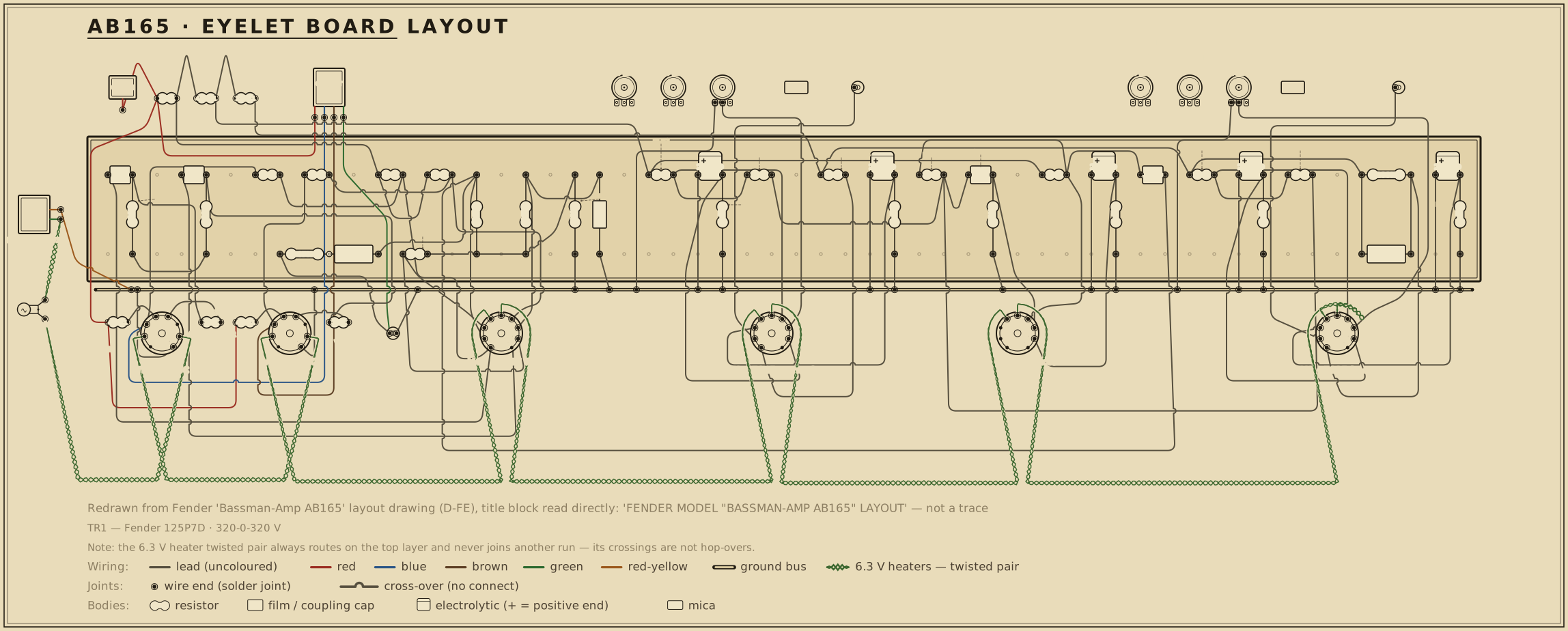
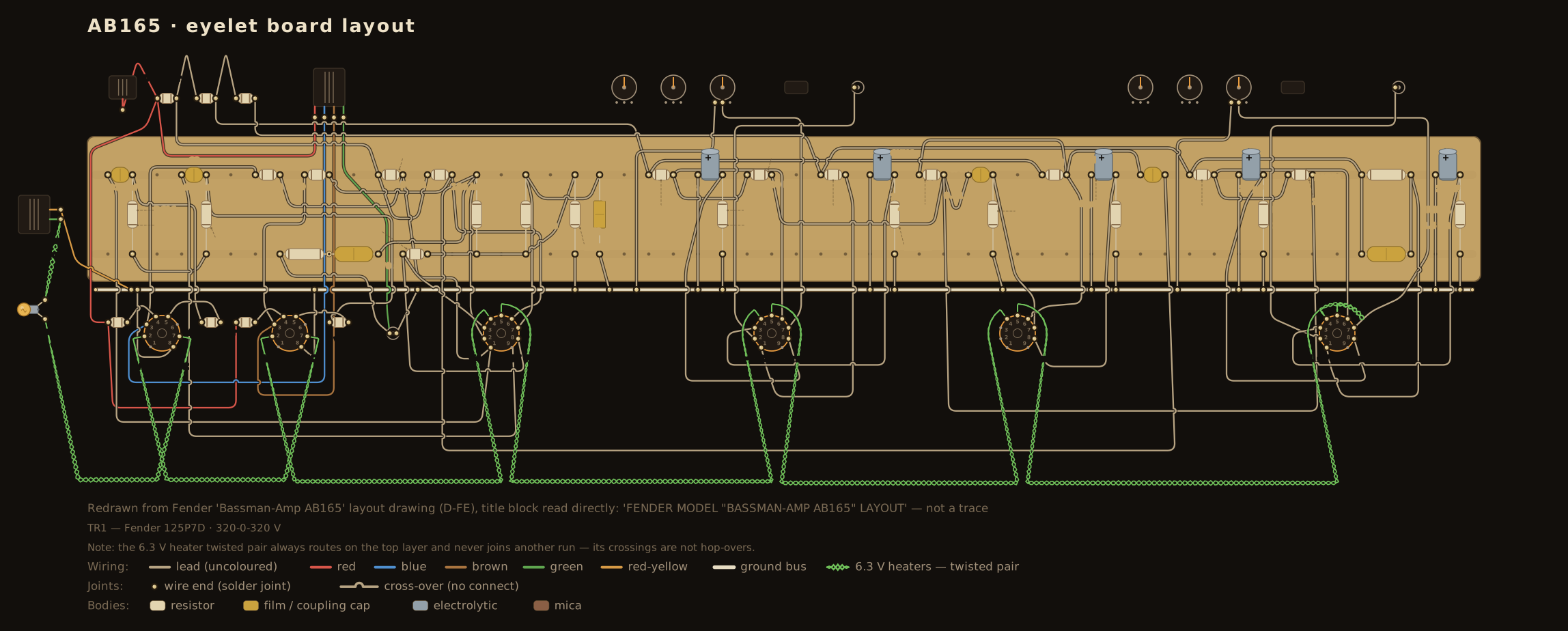
Board layout — redrawn reference diagram · source noted on the drawing Print sheet ↗
AB165 eyelet board layout — an original diagram redrawn from the published layout drawing, showing the principal parts in the order that drawing places them on the board, drawn in the period layout-sheet style with each value lettered on the part.

Scroll the drawing sideways to read the whole board — the source line and the colour legend run along the bottom of the sheet — or open the full-size diagram in its own tab. Values are lettered on the parts in the period shorthand — .02-400, 250-5, 1MEG: how to read it.

Machine-checked wiring. Every modelled part the operating-point netlist places on this board has been verified in CI, terminal for terminal, to be electrically equivalent to the simulated netlist this circuit is verified against. This diagram documents connectivity and part arrangement — it is not a dimensioned 1:1 build template.

Details

The modelled parts are the tube sockets, the plate, cathode and grid-leak resistors, the power-rail droppers, and the coupling and bypass capacitors whose two leads are both named DC nodes; the check proves the same net structure, with no missing or extra connections. Parts outside that DC model — the volume / tone / mixer control-network internals, the negative-bias front end, and the heater chain, pilot lamp and power-transformer / rectifier AC side — are drawn from the cited sources but are not machine-checked; the CI report enumerates every one of their terminals so the boundary is explicit rather than silent.

Board and part positions are drawn at diagram scale, and lead dress, grounding paths, and physical spacing all matter in a high-voltage chassis. If you build from it, verify every connection against the schematic above and the operating-point table below as you go.

Operating point vs. published chart

Chart values read from the published drawing — or, where the drawing carries no voltage chart, from the cited published measurements (never reproduced). The simulated column is this circuit's own netlist solved in ngspice by the run that gates it; every deviation beside it is those two numbers compared, not a separately stated figure. Tolerances are this project's verification targets: tube-pin nodes carry the tolerance the cited source states, or ±20% — the era's printed convention — where it states none, and power rails are held to tighter internal targets. Every gated node lands within target — worst deviation 19.7%.

Node Chart Simulated Deviation Tolerance Note
BPI 415 V 416.1 V 0.3% ±5% phase-inverter supply, +425 through the 1 kOhm-1W dropper
BD 390 V 388.9 V 0.3% ±5% second-stage supply, +415 through the 4.7 kOhm-1W dropper
BC 320 V 305.9 V 4.4% ±8% input-stage supply, +390 through the 27 kOhm-1W dropper — the end of the ladder and the node most sensitive to preamp current
SO1 425 V 424.3 V 0.2% ±8% V5 (6L6GC) screen after its 470 Ohm-1W stopper, off the +425 rail
SO2 425 V 424.3 V 0.2% ±8% V6 (6L6GC) screen after its 470 Ohm-1W stopper
GO1 −45 V −45.0 V 0.0% ±8% V5 grid leak node, fixed bias via 220k-5% from the -45 V line
GO2 −45 V −45.0 V 0.0% ±8% V6 grid leak node
PPIA 225 V 263.3 V 17.0% ±20% PI plate, pin 1 — 100k 5% from +415 with the 220k local feedback resistor from the output plate rail
PPIB 220 V 263.3 V 19.7% ±20% PI plate, pin 6 — the drawing draws both plate loads at 100k 5%, so the 5 V split it prints between the two plates is meter scatter, not circuit asymmetry
KPI 102 V 101.7 V 0.3% ±20% PI joined cathodes (pins 3 and 8), above the 470 Ohm
JPI 100 V 99.6 V 0.4% ±20% PI tail junction (470 Ohm / 22k), both 1M grid leaks return here
PM 250 V 254.2 V 1.7% ±20% V3b plate, 100k from +390
KM 2 V 2.0 V 2.1% ±20% V3b cathode over 1.5k
PB1 220 V 200.7 V 8.8% ±20% V1a plate, 100k from +320 with the 0.01 uF treble-cut shunt across it
KB1 1.6 V 1.6 V 1.4% ±20% V1a cathode over 1.5k
PB2
chart disputed
260 V 208.7 V 19.7% not gated
The sheet draws V1b's 100 kOhm plate load on the +320 V rail (its right-hand corner turns back along that rail …

the +390 V line below it is a separate wire the branch to the normal channel leaves from), and prints +1.8 V at V1b's cathode over 1.5 kOhm. Those two printed numbers give 1.2 mA, which drops 120 V in the printed 100 kOhm and leaves +200 V at the plate, not the printed +260 V; run backwards, +260 V through the same 100 kOhm is 0.6 mA, which over 1.5 kOhm is +0.9 V at the cathode, not the printed +1.8 V. The printed +260 V is the value this stage would carry if it hung on +390 V like the normal channel's identical second stage, which the chart also prints at +260 V. Reported, not gated.

KB2 1.8 V 1.6 V 9.2% ±20% V1b cathode over 1.5k
PN1
chart disputed
280 V 200.7 V 28.3% not gated
V2a is V1a's twin — 100 kOhm plate load, 1.5 kOhm cathode, both drawn on the same +320 V rail — …

yet the chart prints +220 V/+1.6 V on the bass channel and +280 V/+1.9 V on the normal one. The pair moves the wrong way against itself: the higher printed cathode voltage means MORE plate current (1.9 V over 1.5 kOhm = 1.27 mA against 1.6 V = 1.07 mA), and more current through the same 100 kOhm must give a LOWER plate, +193 V rather than the +220 V of its twin — never the +280 V printed. Reported, not gated; the cathode pin beside it (KN1) is gated normally.

KN1 1.9 V 1.6 V 16.9% ±20% V2a cathode over 1.5k
PN2 260 V 251.8 V 3.2% ±20% V2b plate, 100k from +390
KN2 1.9 V 1.9 V 2.2% ±20% V2b cathode over 1.5k

Tube-pin nodes are checked at the tolerance the cited source states, or at the era's ±20% convention where it states none; power-rail nodes are held to tighter internal verification targets. A node marked chart disputed is excluded from that check — its printed value contradicts the rest of the chart, and the note says how; its deviation is shown for the record, not as a result. Simulated figures are the netlist's DC solution, not measurements from a chassis.

The output stage behind these numbers can be drawn: the load line explorer plots this circuit's 6L6GC pair at the DC operating point its netlist carries — 425 V on the plates with a −45 V grid bias — and marks where the load line crosses.

Parts list

Every designator in this list appears on the schematic above, and every designator on the schematic appears here — the two are checked against each other in both directions, a valve's two halves counting as one bottle (V1A and V1B are both V1). The drawing shows one jack symbol per channel input pair; the chassis carries two per channel. The two bias-supply filter cans carry polarity marks but no printed value. The 6L6GC pair is simulated on the 6L6GC model (reference/tubes/6l6gc.yaml).

RefPartValue / ratingRole
R1b Carbon comp resistor 68 kΩ · ½ W Bass input grid stopper (jack 1)
R2b Carbon comp resistor 68 kΩ · ½ W Bass input grid stopper (jack 2)
RGB1 Carbon comp resistor 1 MΩ · ½ W Bass input grid leak
RLB1 Carbon comp resistor 100 kΩ · ½ W V1a plate load
CLB1 Film capacitor 0.01 µF · 400 V Treble-cut shunt across the V1a plate load
RKB1 Carbon comp resistor 1.5 kΩ · ½ W V1a cathode bias
CKB1 Electrolytic capacitor 25 µF · 25 V V1a cathode bypass
CTB Mica capacitor 390 pF Bass-channel treble cap
VRTB Audio-taper potentiometer 250 kΩ-A Bass channel Treble
RSB Carbon comp resistor 100 kΩ · ½ W Bass-channel tone-stack slope resistor
CBB Coupling capacitor 0.1 µF Bass-channel tone-stack bass cap, slope node to the treble-lug/bass node
VRBB Audio-taper potentiometer 250 kΩ-A Bass channel Bass
CBB2 Coupling capacitor 0.1 µF Bass-channel tone-stack middle-leg cap, slope node to the bass-pot foot
RSLB Carbon comp resistor 8.2 kΩ · ½ W Bass-channel tone-stack bleed resistor
CDEEP Coupling capacitor 0.1 µF DEEP cap, tone-stack ladder foot to the switch
SWDEEP Switch SPST DEEP — grounds the extra bass cap
VRVB Audio-taper potentiometer 1 MΩ-A Bass channel Volume
RLB2 Carbon comp resistor 100 kΩ · ½ W V1b plate load (drawn on the +320 V rail — see notes.md)
RKB2 Carbon comp resistor 1.5 kΩ · ½ W V1b cathode bias
CKB2 Electrolytic capacitor 25 µF · 25 V V1b cathode bypass
RMXB Carbon comp resistor 220 kΩ · ½ W Bass channel mixing resistor
R1n Carbon comp resistor 68 kΩ · ½ W Normal input grid stopper (jack 1)
R2n Carbon comp resistor 68 kΩ · ½ W Normal input grid stopper (jack 2)
RGN1 Carbon comp resistor 1 MΩ · ½ W Normal input grid leak
RLN1 Carbon comp resistor 100 kΩ · ½ W V2a plate load
RKN1 Carbon comp resistor 1.5 kΩ · ½ W V2a cathode bias
CKN1 Electrolytic capacitor 25 µF · 25 V V2a cathode bypass
CTN Mica capacitor 250 pF Normal-channel treble cap
VRTN Audio-taper potentiometer 250 kΩ-A Normal channel Treble
RSN Carbon comp resistor 100 kΩ · ½ W Normal-channel tone-stack slope resistor
CBN Coupling capacitor 0.1 µF Normal-channel tone-stack bass cap, slope node to the treble-lug/bass node
VRBN Audio-taper potentiometer 250 kΩ-A Normal channel Bass
CBN2 Coupling capacitor 0.047 µF Normal-channel tone-stack middle-leg cap, slope node to the bleed resistor
RSLN Carbon comp resistor 6.8 kΩ · ½ W Normal-channel tone-stack bleed resistor
CBRN Mica capacitor 120 pF Normal-channel bright cap, volume top lug to wiper
SWBRT Switch SPST BRIGHT — switches the 120 pF across the volume control
VRVN Audio-taper potentiometer 1 MΩ-A Normal channel Volume
RLN2 Carbon comp resistor 100 kΩ · ½ W V2b plate load
RKN2 Carbon comp resistor 1.5 kΩ · ½ W V2b cathode bias
CKN2 Electrolytic capacitor 25 µF · 25 V V2b cathode bypass
RMXN Carbon comp resistor 220 kΩ · ½ W Normal channel mixing resistor
RFBM Carbon comp resistor 470 kΩ · ½ W V3b plate back to the mixing node — the AB165 blend/feedback resistor
CMIX Film capacitor 0.01 µF · 400 V Mixing node → V3b grid coupling
RGM Carbon comp resistor 470 kΩ · ½ W V3b grid leak
RLM Carbon comp resistor 100 kΩ · ½ W V3b plate load
RKM Carbon comp resistor 1.5 kΩ · ½ W V3b cathode bias
CKM Electrolytic capacitor 25 µF · 25 V V3b cathode bypass
CPIA Coupling capacitor 0.1 µF · 400 V V3b plate → PI hot grid
RLPA Carbon comp resistor 100 kΩ · ½ W · 5% PI plate load (hot side)
RLPB Carbon comp resistor 100 kΩ · ½ W · 5% PI plate load (cold side)
RGPA Carbon comp resistor 1 MΩ · ½ W PI grid leak (hot), returned to the tail junction
RGPB Carbon comp resistor 1 MΩ · ½ W PI grid leak (cold), returned to the tail junction
RTAIL Carbon comp resistor 470 Ω · ½ W PI cathode resistor
RT2 Carbon comp resistor 22 kΩ · ½ W PI tail (junction → ground)
CPIB Film capacitor 0.1 µF · 200 V PI cold-grid AC ground
RBSA Carbon comp resistor 220 kΩ · ½ W Local feedback, V5 plate → PI hot plate
RBSB Carbon comp resistor 220 kΩ · ½ W Local feedback, V6 plate → PI cold plate
C1 Film capacitor 0.022 µF · 400 V PI hot plate → V5 grid
C2 Film capacitor 0.022 µF · 400 V PI cold plate → V6 grid
RGL1 Carbon comp resistor 220 kΩ · ½ W · 5% V5 grid leak, from the −45 V bias line
RGL2 Carbon comp resistor 220 kΩ · ½ W · 5% V6 grid leak, from the −45 V bias line
RGS1 Carbon comp resistor 1.5 kΩ · ½ W V5 grid stopper
RGS2 Carbon comp resistor 1.5 kΩ · ½ W V6 grid stopper
RS1 Wirewound resistor 470 Ω · 1 W V5 screen resistor
RS2 Wirewound resistor 470 Ω · 1 W V6 screen resistor
TR3 Output transformer Fender 125A13A Push-pull 6L6GC output
RNFB Carbon comp resistor 47 kΩ · ½ W Negative feedback, speaker line → PI hot grid (DC-blocked)
CNFB Coupling capacitor 0.1 µF · 400 V Negative-feedback series capacitor
TR1 Power transformer Fender 125P7D · 320-0-320 V HT + heaters (export model 125P7DX)
TR2 Filter choke Fender 125C1A Reservoir → screen rail
D1 Rectifier diode silicon (×3 in series) HT rectifier, upper leg
D2 Rectifier diode silicon (×3 in series) HT rectifier, lower leg
SWSTBY Switch SPST Standby — breaks the HT rail ahead of the choke
C10 Electrolytic capacitor 70 µF · 350 V Reservoir filter, upper half of the series pair
C11 Electrolytic capacitor 70 µF · 350 V Reservoir filter, lower half of the series pair
RBAL1 Carbon comp resistor 220 kΩ · 1 W Reservoir balancing resistor (upper)
RBAL2 Carbon comp resistor 220 kΩ · 1 W Reservoir balancing resistor (lower)
C12 Electrolytic capacitor 20 µF · 525 V Filter, screen node (+425, after the choke)
RD1 Carbon comp resistor 1 kΩ · 1 W Rail dropper, screen node → phase-inverter node
C13 Electrolytic capacitor 20 µF · 525 V Filter, phase-inverter node (+415)
RD2 Carbon comp resistor 4.7 kΩ · 1 W Rail dropper, +415 → second-stage node
C14 Electrolytic capacitor 20 µF · 525 V Filter, second-stage node (+390)
RD3 Carbon comp resistor 27 kΩ · 1 W Rail dropper, +390 → input-stage node
C15 Electrolytic capacitor 8 µF · 450 V Filter, input-stage node (+320)
RBIAS Wirewound resistor 470 Ω · 1 W Bias-supply series resistor off the HT winding
DBIAS Rectifier (bias) silicon diode Bias-supply rectifier
CB1 Electrolytic capacitor electrolytic (value not printed) Bias-supply filter
CB2 Electrolytic capacitor electrolytic (value not printed) Bias-supply filter
RBB1 Carbon comp resistor 10 kΩ · ½ W Bias divider, balance-pot end (V5 side)
RBB2 Carbon comp resistor 10 kΩ · ½ W Bias divider, balance-pot end (V6 side)
RBB3 Carbon comp resistor 15 kΩ · ½ W Bias divider foot to ground
VRBAL Linear potentiometer 10 kΩ-L BIAS BALANCE — the sheet's 'hum balance' control
SWAC Switch SPST AC switch
F1 Fuse 2 A slo-blo Mains fuse
SWGND Switch SPDT Ground switch (period; not in modern builds)
CDEATH Ceramic capacitor 0.047 µF · 600 V Ground-switch cap (period; not in modern builds)
V1 Preamp tube 12AX7 (7025) Bass channel input + second stage (V1a/V1b)
V2 Preamp tube 12AX7 (7025) Normal channel input + second stage (V2a/V2b)
V3 Preamp tube 12AX7 (7025) Mixer/driver stage (V3b)
V4 Preamp/driver tube 12AT7 Long-tailed-pair phase inverter
V5 Power tube 6L6GC Push-pull output (hot side)
V6 Power tube 6L6GC Push-pull output (cold side)

Circuit story

The best-known blackface Bassman: a 50-watt piggyback head on a pair of 6L6GC output tubes, solid-state rectified, with two channels — Bass and Normal — that meet at a shared mixing node instead of at the phase inverter. It shares its name with the tweed 4x10 Bassman and almost nothing else. Where the 5F6-A is a guitar amplifier that happened to be sold for bass, the AB165 is the purpose-built bass head Fender went back and designed, and its voicing says so: the Bass channel opens with a 0.01 µF capacitor thrown straight across its first plate load.

The drawing letters the three preamp bottles 7025, the low-noise selected 12AX7; the inverter is a 12AT7.

Signal path

Bass channel. Two inputs (68 kΩ stoppers on a 1 MΩ leak) → a 12AX7 stage with a 100 kΩ plate load, a 1.5 kΩ/25 µF cathode, and the 0.01 µF treble cut across the plate load → a two-knob tone stack (100 kΩ slope, a 390 pF treble cap, 250 kΩ Treble and Bass, 8.2 kΩ foot) with a DEEP switch that grounds a further 0.1 µF at the foot of the ladder → a 1 MΩ Volume → a second 12AX7 stage (100 kΩ plate, 1.5 kΩ cathode).

Normal channel. The same front end without the plate-load capacitor, a 250 pF treble cap, a 0.047 µF middle-leg cap and a 6.8 kΩ foot, and a BRIGHT switch that bridges 120 pF from the volume pot's top lug to its wiper. Then its own second 12AX7 stage, identical part for part to the bass channel's.

Mixer. Both second-stage plates reach one node through 220 kΩ each, and that node is coupled by 0.01 µF into a third 12AX7 (100 kΩ plate, 1.5 kΩ cathode, 470 kΩ grid leak) whose plate is returned to the same node through 470 kΩ. Mixing before the driver, rather than at the inverter's grid, is what lets one blend control sit ahead of a single gain stage.

Phase inverter and output. A 12AT7 long-tailed pair with two 100 kΩ 5 % plate loads, a 470 Ω cathode resistor to a tail junction, a 22 kΩ tail to ground bypassed by 0.1 µF, and both 1 MΩ grid leaks returned to that junction. Its cold grid is tied to ground for AC; the 47 kΩ negative-feedback resistor comes back from the speaker line into the hot grid through a 0.1 µF capacitor, mixing with the signal rather than entering at the tail.

Each inverter plate also carries a 220 kΩ straight back to the output tube it drives — local feedback wrapped around the coupling capacitor and the output stage. It is the AB165's signature and the part most often removed by people converting these heads to the earlier AA864 arrangement. It is not cosmetic: it sets the inverter's operating point as much as its plate loads do. With the two 220 kΩ resistors in place the simulated inverter cathode sits at +101.7 V against a printed +102 V; without them the same stage cannot reach much past +67 V. That agreement is the strongest single check on this reading of the sheet.

The 6L6GC pair is fixed-biased at −45 V through 220 kΩ 5 % leaks and 1500 Ω stoppers, with 470 Ω · 1 W screen resistors and grounded cathodes. The bias line is trimmed by a 10 kΩ-L balance control — the sheet's "hum balance", the one the notice tells you to reset when you fit new bottles — with 10 kΩ to each end and 15 kΩ to ground. Simulated idle is about 37 mA per plate at +425 V, near 16 W, a little over half the 6L6GC's rating.

Power

320-0-320 V (TR1 125P7D; 125P7DX on the export model) → three series silicon diodes per leg → +425 V across two 70 µF · 350 V cans in series with 220 kΩ · 1 W balancing → standby switch → the 125C1A choke → +425 V at the screens → 1 kΩ · 1 W → +415 V at the inverter → 4.7 kΩ · 1 W → +390 V at the second stages and the driver → 27 kΩ · 1 W → +320 V at the two channel inputs. The netlist drives only the first of those and solves the rest through the drawing's own droppers, so the printed ladder is a checked claim: +415 and +390 land within half a percent of print, +320 within five.

A separate negative supply — 470 Ω · 1 W off the HT winding, a silicon diode and two filter cans — feeds the bias divider.

Reading against the printed chart

The drawing prints a full voltage chart at ±20 %, read to ground with an electronic voltmeter. Most of it verifies closely: the supply ladder, the screens at +425 V, the bias line at −45 V, the inverter's +102 V / +100 V cathode and tail, the driver at +250 V / +2.0 V, the normal channel's second stage at +260 V / +1.9 V, and the bass channel's input stage at +220 V / +1.6 V. The worst gated nodes are the two inverter plates, which simulate about 263 V against a printed +225 V and +220 V — inside the sheet's own ±20 %, but only just, and the two printed plate values differ by 5 V on plate loads the drawing gives as identical 100 kΩ 5 % parts.

Two printed plate voltages are reported rather than compared, because each contradicts the drawing's own numbers rather than this simulation's:

  • The normal channel's input plate, printed +280 V. V2a is V1a's twin — 100 kΩ plate load, 1.5 kΩ cathode, both hung on the same +320 V rail — but the chart prints +220 V / +1.6 V on one and +280 V / +1.9 V on the other. The pair moves the wrong way against itself: the higher cathode voltage is more current (1.9 V over 1.5 kΩ is 1.27 mA against 1.07 mA), and more current through the same 100 kΩ has to leave a lower plate, near +193 V — never +280 V.

  • The bass channel's second-stage plate, printed +260 V. Here the contradiction is in the wiring. The sheet takes this stage's 100 kΩ load down to the +320 V rail — its corner turns back along that rail, and the +390 V line below it is a separate wire, the one the normal channel's identical second stage branches from. On +320 V the printed +1.8 V cathode gives 1.2 mA and a +200 V plate; the printed +260 V would need 0.6 mA, which over 1.5 kΩ is +0.9 V, not +1.8 V. On +390 V the same parts give +268 V — the value the chart prints, and the value it also prints for the normal channel's second stage. The likeliest reading is a drafting slip in the rail routing, but this corpus documents the drawing as drawn: the netlist keeps the load on +320 V, and the printed +260 V is carried as a disputed node with the arithmetic above rather than quietly rewired to make it fit.

Everything else in the chart is gated at the sheet's own ±20 % convention, and this circuit is published as verified on that basis — nineteen nodes compared, the worst of them the inverter plate pair above.

Lineage

The AB165 is the second revision letter on the blackface piggyback chassis, and this corpus documents the circuit it supersedes: the AA864 of 1964, whose Bass/Normal split, 12AT7 long-tailed pair, solid-state supply and fixed-bias 6L6GC pair all carry straight through. What the AB165 changes is the Bass channel — the blend network and the 220 kΩ local feedback from each output plate that give this revision its reputation. Behind the AA864 stands the blonde 6G6-B piggyback, also documented here.

None of it comes from the tweed Bassman. The 5F6-A shares the name and nothing in this schematic.

Sources