AA864 (Bassman-style) Blackface Bassman‑style · 1964–1965 · 50 W

✓ verified 2026-08-13
Schematic — redrawn in KiCad · scroll to zoom, drag to pan
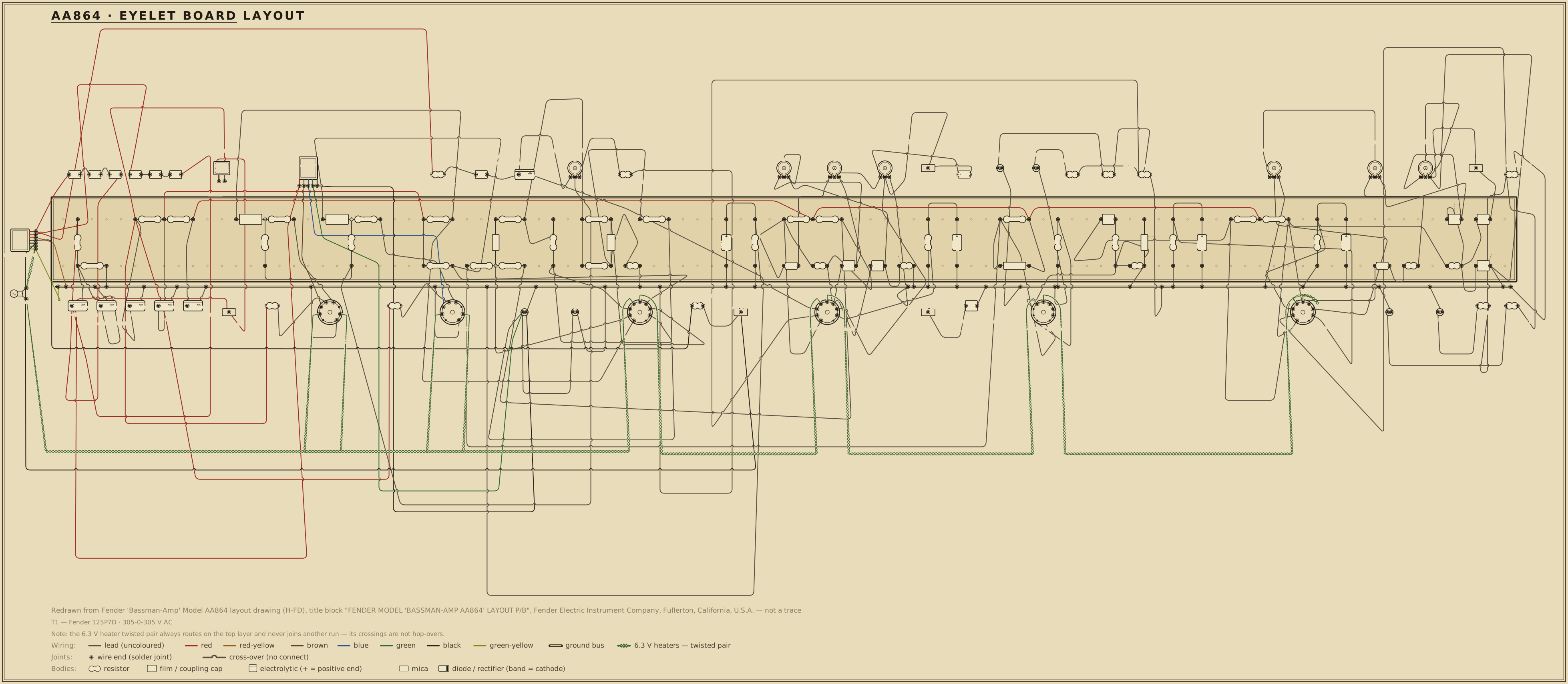
Board layout — redrawn reference diagram · source noted on the drawing Print sheet ↗
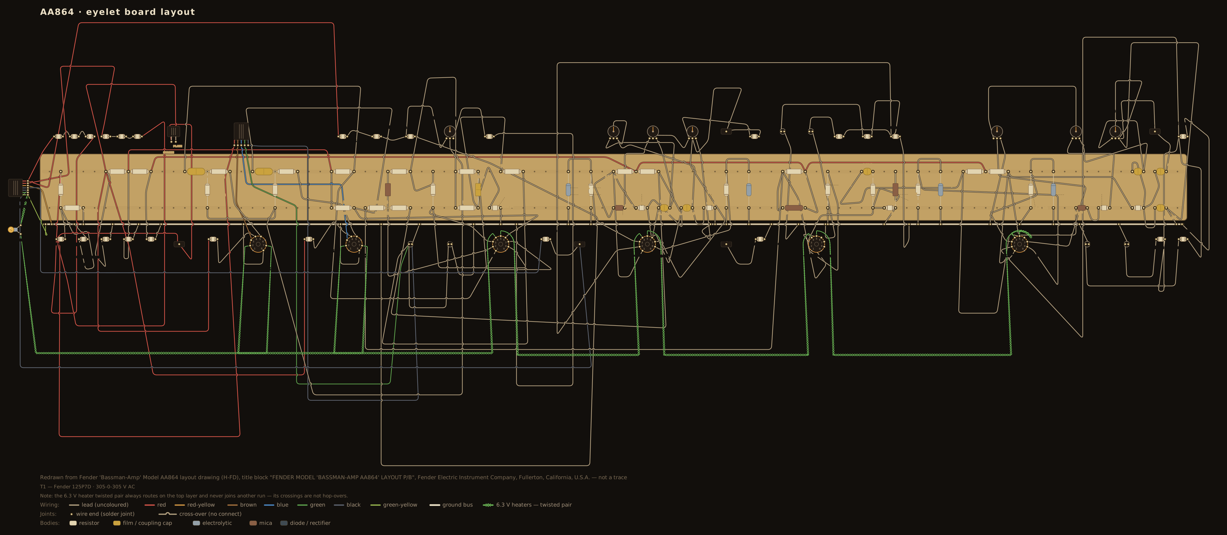
AA864 (Bassman-style) eyelet board layout — an original diagram redrawn from the published layout drawing, showing the principal parts in the order that drawing places them on the board, drawn in the period layout-sheet style with each value lettered on the part.

Scroll the drawing sideways to read the whole board — the source line and the colour legend run along the bottom of the sheet — or open the full-size diagram in its own tab. Values are lettered on the parts in the period shorthand — .02-400, 250-5, 1MEG: how to read it.

Machine-checked wiring. Every modelled part the operating-point netlist places on this board has been verified in CI, terminal for terminal, to be electrically equivalent to the simulated netlist this circuit is verified against. This diagram documents connectivity and part arrangement — it is not a dimensioned 1:1 build template.

Details

The modelled parts are the tube sockets, the plate, cathode and grid-leak resistors, the power-rail droppers, and the coupling and bypass capacitors whose two leads are both named DC nodes; the check proves the same net structure, with no missing or extra connections. Parts outside that DC model — the volume / tone / mixer control-network internals, the negative-bias front end, and the heater chain, pilot lamp and power-transformer / rectifier AC side — are drawn from the cited sources but are not machine-checked; the CI report enumerates every one of their terminals so the boundary is explicit rather than silent.

Board and part positions are drawn at diagram scale, and lead dress, grounding paths, and physical spacing all matter in a high-voltage chassis. If you build from it, verify every connection against the schematic above and the operating-point table below as you go.

Operating point vs. published chart

Chart values read from the published drawing — or, where the drawing carries no voltage chart, from the cited published measurements (never reproduced). The simulated column is this circuit's own netlist solved in ngspice by the run that gates it; every deviation beside it is those two numbers compared, not a separately stated figure. Tolerances are this project's verification targets: tube-pin nodes carry the tolerance the cited source states, or ±20% — the era's printed convention — where it states none, and power rails are held to tighter internal targets. Every gated node lands within target — worst deviation 11.6%.

Node Chart Simulated Deviation Tolerance Note
S61 420 V 419.2 V 0.2% ±8% 6L6GC (V5) screen after its 470 Ohm-1W stopper, off the +420 screen rail
G61 −44 V −44.0 V 0.0% ±8% 6L6GC (V5) grid, fixed bias via 220k from the -44 V supply, through the 1.5k stopper
BPI 410 V 409.6 V 0.1% ±5% phase-inverter plate rail, derived from the driven +420 screen rail through the drawn 1 kOhm-1W dropper
BPR 380 V 379.4 V 0.2% ±20% Preamp rail, below the 4.7 kOhm-1W dropper. The two published sheets print two different figures at this node and only one of them closes. The LAYOUT sheet marks the eyelet that feeds the preamp plate loads +380 V; the circuit sheet marks the same node +340 V. Take the circuit sheet's figure and the drawn resistor must pass (410-340)/4.7k = 14.9 mA, but the only load is five 100 kOhm-loaded preamp triodes. Take the layout sheet's and the arithmetic closes: (380-235)/100k + (380-235)/100k + (380-250)/100k + (380-250)/100k + (380-240)/100k = 6.90 mA, a 32 V drop, putting the node at +378 V. The entry therefore carries the layout sheet's +380 V and records the circuit sheet's +340 V as the figure that does not close.
PB1 235 V 250.6 V 6.6% ±20% Bass channel input plate (V1a), 100k from the preamp rail
KB1 2 V 1.9 V 3.4% ±20% Bass channel input cathode over 1.5k (25 uF bypass)
PB2 235 V 250.6 V 6.6% ±20% Bass channel 2nd-stage plate (V1b), 100k from the preamp rail
KB2 2 V 1.9 V 3.4% ±20% Bass channel 2nd-stage cathode over 1.5k (25 uF bypass)
PB3 240 V 250.6 V 4.4% ±20% Bass channel driver plate (V3b), 100k with 0.005 uF across it
KB3 1.9 V 1.9 V 1.7% ±20% Bass channel driver cathode over 1.5k — the one preamp cathode with no bypass can
PN1 250 V 250.6 V 0.2% ±20% Normal channel input plate (V2a), 100k from the preamp rail
KN1 1.8 V 1.9 V 7.3% ±20% Normal channel input cathode over 1.5k (25 uF bypass)
PN2 250 V 250.6 V 0.2% ±20% Normal channel 2nd-stage plate (V2b), 100k from the preamp rail
KN2 1.8 V 1.9 V 7.3% ±20% Normal channel 2nd-stage cathode over 1.5k (25 uF bypass)
PPA 220 V 234.9 V 6.8% ±20% PI plate, 82k (hot) side
PPB 205 V 228.8 V 11.6% ±20% PI plate, 100k (cold) side
KPI 95 V 88.9 V 6.4% ±20% PI joined cathodes, above the 470 Ohm
JPI 93 V 87.1 V 6.4% ±20% PI tail junction (470 Ohm / 22k), grid-leak return
NFB 0.4 V negative-feedback node — the 22k tail's return, working into the 100 Ohm to ground. Not printed on the chart; reported for information

Tube-pin nodes are checked at the tolerance the cited source states, or at the era's ±20% convention where it states none; power-rail nodes are held to tighter internal verification targets. Simulated figures are the netlist's DC solution, not measurements from a chassis.

The output stage behind these numbers can be drawn: the load line explorer plots this circuit's 6L6GC pair at the DC operating point its netlist carries — 422 V on the plates with a −44 V grid bias — and marks where the load line crosses.

Parts list

Every designator in this list appears on the schematic above, and every designator on the schematic appears here — the two are checked against each other in both directions, a valve's two halves counting as one bottle (V1A and V1B are both V1). The drawing shows one jack pair per channel; the chassis carries two jacks per channel. Three 7025 bottles supply six triode sections and the circuit uses five — the Bass channel takes three stages and the Normal channel two — so one section is unused; the sheet does not say which bottle carries it. The tone stacks differ between channels: the Normal channel draws the blackface two-knob ladder (100 kΩ slope + 250 pF off the plate, 0.1 µF to the treble-lug/bass node, bass rheostat over the 0.047 µF / 6.8 kΩ foot), while the Bass channel draws the same ladder with a 250 kΩ resistor above a 50 kΩ treble pot, a 10 kΩ bass pot, three 0.1 µF caps off the slope node instead of the Normal channel's 0.1 / 0.047 pair, and a Deep switch that parallels the third of them into the grounded foot.

RefPartValue / ratingRole
R1b Carbon comp resistor 68 kΩ · ½ W Bass input grid stopper (jack 1)
R2b Carbon comp resistor 68 kΩ · ½ W Bass input grid stopper (jack 2)
RGB1 Carbon comp resistor 1 MΩ · ½ W Bass input grid leak
RLB1 Carbon comp resistor 100 kΩ · ½ W V1a plate load
RKB1 Carbon comp resistor 1.5 kΩ · ½ W V1a cathode bias
CKB1 Electrolytic capacitor 25 µF · 25 V V1a cathode bypass
CTB Mica capacitor 250 pF Bass-channel treble cap, off the V1a plate
RTB Carbon comp resistor 250 kΩ · ½ W Bass-channel treble series resistor, above the treble pot
VRTB Potentiometer 50 kΩ-A Bass-channel treble
RSB1 Carbon comp resistor 100 kΩ · ½ W Bass-channel slope resistor, plate to the ladder node
CBB1 Coupling capacitor 0.1 µF Bass-channel ladder cap, slope node to the treble-lug/bass-top junction
CBB2 Coupling capacitor 0.1 µF Bass-channel ladder cap, slope node to the bass-pot foot
CBB3 Coupling capacitor 0.1 µF Bass-channel Deep cap, switched in parallel with CBB2
SWDEEP Toggle switch SPST Deep switch — parallels CBB3 into the ladder foot
VRBB Potentiometer 10 kΩ-A Bass-channel bass (rheostat in the ladder)
VRVB Audio-taper potentiometer 250 kΩ-A Bass-channel volume
RLB2 Carbon comp resistor 100 kΩ · ½ W V1b plate load
RKB2 Carbon comp resistor 1.5 kΩ · ½ W V1b cathode bias
CKB2 Electrolytic capacitor 25 µF · 25 V V1b cathode bypass
CCB2 Coupling capacitor 0.1 µF V1b plate → driver grid divider
RDV1 Carbon comp resistor 220 kΩ · ½ W Driver grid divider, series leg
RDV2 Carbon comp resistor 220 kΩ · ½ W Driver grid divider, shunt leg
CDV Mica capacitor 0.001 µF Driver grid divider shunt cap, across RDV2
RLB3 Carbon comp resistor 100 kΩ · ½ W Driver plate load
CLB3 Mica capacitor 0.005 µF Driver plate-load bypass — treble roll-off across RLB3
RKB3 Carbon comp resistor 1.5 kΩ · ½ W Driver cathode bias (no bypass capacitor)
RMXB Carbon comp resistor 220 kΩ · ½ W Bass-channel mix resistor into the phase-inverter grid node
R1n Carbon comp resistor 68 kΩ · ½ W Normal input grid stopper (jack 1)
R2n Carbon comp resistor 68 kΩ · ½ W Normal input grid stopper (jack 2)
RGN1 Carbon comp resistor 1 MΩ · ½ W Normal input grid leak
RLN1 Carbon comp resistor 100 kΩ · ½ W V2a plate load
RKN1 Carbon comp resistor 1.5 kΩ · ½ W V2a cathode bias
CKN1 Electrolytic capacitor 25 µF · 25 V V2a cathode bypass
CTN Mica capacitor 250 pF Normal treble cap, off the V2a plate
VRTN Potentiometer 250 kΩ-A Normal treble
RSN Carbon comp resistor 100 kΩ · ½ W Normal tone-stack slope resistor
CBN Coupling capacitor 0.1 µF Normal tone-stack bass cap, slope node to the bass pot
VRBN Potentiometer 250 kΩ-A Normal bass (rheostat in the ladder)
CBN2 Coupling capacitor 0.047 µF Normal tone-stack middle-leg cap, slope node to the bleed resistor
RSLN Carbon comp resistor 6.8 kΩ · ½ W Normal tone-stack bleed resistor
VRVN Audio-taper potentiometer 1 MΩ-A Normal volume
CBRN Mica capacitor 120 pF Normal bright cap, across the volume pot (top lug to wiper)
SWBRT Toggle switch SPST Bright switch — puts CBRN across the volume pot
RLN2 Carbon comp resistor 100 kΩ · ½ W V2b plate load
RKN2 Carbon comp resistor 1.5 kΩ · ½ W V2b cathode bias
CKN2 Electrolytic capacitor 25 µF · 25 V V2b cathode bypass
RMXN Carbon comp resistor 220 kΩ · ½ W Normal-channel mix resistor into the phase-inverter grid node
CPI Mica capacitor 500 pF Mix node → PI hot-grid coupling
RLPA Carbon comp resistor 82 kΩ · ½ W · 5% PI plate load (hot side)
RLPB Carbon comp resistor 100 kΩ · ½ W · 5% PI plate load (cold side)
RGPA Carbon comp resistor 1 MΩ · ½ W PI grid leak (hot), returned to the tail junction
RGPB Carbon comp resistor 1 MΩ · ½ W PI grid leak (cold), returned to the tail junction
RTAIL Carbon comp resistor 470 Ω · ½ W PI cathode resistor
RT2 Carbon comp resistor 22 kΩ · ½ W PI tail (junction → feedback node)
RNF Carbon comp resistor 100 Ω · ½ W Feedback node → ground; the tail's return and the NFB divider foot
RNFB Carbon comp resistor 820 Ω · ½ W Negative feedback, OT secondary → feedback node (DC-neutral)
CPIB Coupling capacitor 0.1 µF · 200 V Feedback node → PI cold grid
C1 Coupling capacitor 0.1 µF · 400 V PI hot plate → V5 grid
C2 Coupling capacitor 0.1 µF · 400 V PI cold plate → V6 grid
RGL1 Carbon comp resistor 220 kΩ · ½ W · 5% V5 grid leak, from the −44 V bias line
RGL2 Carbon comp resistor 220 kΩ · ½ W · 5% V6 grid leak, from the −44 V bias line
RGS1 Carbon comp resistor 1.5 kΩ · ½ W V5 grid stopper
RGS2 Carbon comp resistor 1.5 kΩ · ½ W V6 grid stopper
RS1 Wirewound resistor 470 Ω · 1 W V5 screen resistor
RS2 Wirewound resistor 470 Ω · 1 W V6 screen resistor
T3 Output transformer Fender 125A13A Push-pull 6L6GC output, into the 2x12 cabinet + EXT SPKR jack
T1 Power transformer Fender 125P7D · 305-0-305 V AC HT + heaters + pilot (export model: 125P7DX)
T2 Filter choke Fender 125C1A Plate rail → screen rail
D1 Rectifier diode silicon HT rectifier, upper phase (1 of 3 in series)
D2 Rectifier diode silicon HT rectifier, upper phase (2 of 3 in series)
D3 Rectifier diode silicon HT rectifier, upper phase (3 of 3 in series)
D4 Rectifier diode silicon HT rectifier, lower phase (1 of 3 in series)
D5 Rectifier diode silicon HT rectifier, lower phase (2 of 3 in series)
D6 Rectifier diode silicon HT rectifier, lower phase (3 of 3 in series)
C10 Electrolytic capacitor 70 µF · 350 V Reservoir, upper half of the series pair (+422 V node)
C11 Electrolytic capacitor 70 µF · 350 V Reservoir, lower half of the series pair
RBL1 Wirewound resistor 220 kΩ · 1 W Reservoir balancing resistor, across C10
RBL2 Wirewound resistor 220 kΩ · 1 W Reservoir balancing resistor, across C11
SWSTBY Toggle switch SPST Standby — +422 V reservoir to the plate rail / choke input
C12 Electrolytic capacitor 20 µF · 525 V Filter, screen rail (+420 V, past the choke)
RD1 Wirewound resistor 1 kΩ · 1 W Rail dropper, screens → phase-inverter rail
C13 Electrolytic capacitor 20 µF · 525 V Filter, phase-inverter rail (+410 V)
RD2 Wirewound resistor 4.7 kΩ · 1 W Rail dropper, phase-inverter rail → preamp rail
C14 Electrolytic capacitor 20 µF · 525 V Filter, preamp rail (+380 V on the layout sheet — see voltages.yaml)
RBIAS Wirewound resistor 470 Ω · 1 W Bias-supply series resistor, off the 305 V AC tap
DBIAS Rectifier diode silicon Bias-supply rectifier
CB1 Electrolytic capacitor 25 µF · 50 V Bias-supply filter
VRBIAS Linear potentiometer 10 kΩ-L Bias adjust — wiper feeds the 220 kΩ grid leaks
RBIAS2 Carbon comp resistor 15 kΩ · ½ W Bias divider, pot to ground
FUSE Fuse 2 A slo-blo Mains fuse
SWAC Toggle switch SPST AC switch
SWGND Toggle switch SPDT Ground switch (period; not in modern builds)
CDEATH Ceramic capacitor 0.047 µF · 600 V Ground-switch cap (period; not in modern builds)
V1 Preamp tube 7025 Bass channel input + 2nd stage (V1a/V1b)
V2 Preamp tube 7025 Normal channel input + 2nd stage (V2a/V2b)
V3 Preamp tube 7025 Bass channel driver (V3b); one triode section is unused
V4 Preamp/driver tube 12AT7 Long-tailed-pair phase inverter
V5 Power tube 6L6GC Push-pull output (hot side)
V6 Power tube 6L6GC Push-pull output (cold side)

Circuit story

Two amplifiers have carried the Bassman name. The first was a tweed combo that guitarists took over, ending in the 5F6-A: four ten-inch speakers, a cathode-follower tone stack and the circuit Marshall's first head was built around. The AA864 is the other one. Black Tolex, a piggyback head over its own cabinet, solid-state rectification, fifty watts, and a front panel that says Bass Instrument on one channel — Fender going back to building a bass amplifier after the name had spent a decade attached to a guitar classic. The two share the word on the panel and nothing else. The title block reads FENDER MODEL "BASSMAN-AMP AA864" P/B.

What the AA864 does inherit, it inherits from the blonde piggyback it replaced — the 6G6-B, also documented here: the two-channel Bass/Normal split, the solid-state supply and the long-tailed-pair inverter all carry across the changeover, and the preamp is redesigned around them. A year later the AB165 reworks the Bass channel again on the same chassis.

Six bottles do the work: three 7025s (the low-noise 12AX7 the sheet calls for), a 12AT7 phase inverter, and a 6L6GC pair. The three 7025s hold six triode sections and the circuit uses five, because the two channels are not built the same.

Two channels, two different amplifiers

Normal is the ordinary blackface channel: two gain stages either side of the familiar two-knob stack. Bass Instrument gets a third gain stage and a tone network with an extra rung — the channel the amp is named for, and the one the panel puts first.

Normal. Two jacks on 68 kΩ stoppers and a shared 1 MΩ leak → V2a (100 kΩ plate load, 1.5 kΩ cathode, 25 µF bypass) → the blackface treble/bass ladder: a 250 pF treble cap and a 100 kΩ slope resistor both off the plate, 0.1 µF from the slope foot to the treble-lug/bass junction, a 250 kΩ bass rheostat down onto a 0.047 µF / 6.8 kΩ leg, output taken at the 250 kΩ treble wiper → a 1 MΩ volume with a switched 120 pF Bright cap across it → V2b, an identical 100 kΩ / 1.5 kΩ stage → 220 kΩ into the inverter's grid node.

Bass Instrument. Same input arrangement into V1a, then the same ladder scaled for the low end. The treble cap is still 250 pF, but it feeds a 250 kΩ series resistor above a 50 kΩ treble pot, so the control moves a small window of a much larger divider. The slope resistor is still 100 kΩ, and off its foot hang three 0.1 µF capacitors where the Normal channel has a 0.1 and a 0.047: one across to the treble-lug/bass junction, one down into the grounded foot, and a third that the Deep switch parallels with it — doubling the capacitance the bass control works against. The rheostat in the ladder is a 10 kΩ pot rather than 250 kΩ, and there is no 6.8 kΩ leg: the foot goes straight to ground. A 250 kΩ volume follows, then V1b (100 kΩ / 1.5 kΩ / 25 µF).

The extra stage is where the channel earns its name. V1b's plate hands 0.1 µF to a 220 kΩ / 220 kΩ divider with 0.001 µF across its foot — a deliberate 2:1 pad that rolls off above about 1.5 kHz — and that feeds V3b, a third 100 kΩ / 1.5 kΩ stage whose cathode resistor is the only one on the sheet with no bypass capacitor, and whose plate load carries 0.005 µF straight across it, a corner near 800 Hz. Attenuate, amplify again with local degeneration, then roll the top off at the plate: gain restored without the brightness that would come with it. V3b's plate then meets the Normal channel through its own 220 kΩ.

Phase inverter

Both channels' 220 kΩ mix resistors land on one node, and 500 pF carries it into the 12AT7 long-tailed pair — 82 kΩ on the hot plate, 100 kΩ on the cold, both 5 %, from the +410 V rail; a 470 Ω resistor under the joined cathodes and a 22 kΩ tail; 1 MΩ grid leaks returned to the tail junction, which the chart puts at +93 V under +95 V cathodes.

The tail does not go to ground. It returns to a 100 Ω resistor, and the amplifier's global feedback — 820 Ω from the output transformer's secondary — lands on the same node, so the feedback voltage develops across that 100 Ω. A 0.1 µF · 200 V capacitor carries the node to the cold grid, which takes its DC from the tail junction through its 1 MΩ leak.

Output

0.1 µF couplers into 220 kΩ · 5 % grid leaks returned to the −44 V bias line, then 1.5 kΩ grid stoppers, into the 6L6GC pair: cathodes to ground, screens off the +420 V rail through 470 Ω · 1 W stoppers, plates printed at +420 V into the 125A13A transformer, whose centre tap the sheet marks +422 V, and out to the cabinet's two speakers, with an EXT SPKR jack in parallel.

Power

No rectifier tube. TR1 (125P7D; 125P7DX on the export model) runs 305-0-305 V AC into two strings of three series silicon diodes — stacked for reverse voltage, not for current — giving +422 V across two 70 µF · 350 V cans in series, balanced by a pair of 220 kΩ · 1 W resistors. A standby switch passes that to the plate rail, which feeds the output transformer's centre tap at the same +422 V; the 125C1A choke drops it to +420 V for the screens, 1 kΩ · 1 W to +410 V for the inverter, and 4.7 kΩ · 1 W to the preamp rail, with a 20 µF · 525 V can on each. The bias supply taps the same 305 V winding through 470 Ω · 1 W and one diode into a 25 µF · 50 V can, then a 10 kΩ linear bias adjust over a 15 kΩ leg, out at −44 V.

Reading against the printed chart

The drawing prints a full voltage chart — every value at ±20 %, read to ground with an electronic voltmeter. Two rails are supplied to the simulation, the +422 V plate rail and the +420 V screen rail either side of the choke; everything below is solved through the drawing's own droppers.

Most of it lands close. The inverter rail solves to +410 V against a printed +410 V. The screens sit at +419 V against +420 V. Every preamp plate solves to +251 V — right on the Normal channel's printed +250 V, and 5–7 % above the Bass channel's printed +235 V — with cathodes at +1.93 V against printed values of +2.0, +1.8 and +1.9 V. The inverter reads +235 V and +229 V at its plates against printed +220 and +205 V, with +89 V cathodes and a +87 V tail junction against +95 and +93 V. The worst node is about 12 % out, inside the sheet's own tolerance.

One node is printed twice, differently. The circuit sheet marks the preamp rail — the node below the 4.7 kΩ · 1 W dropper — +340 V. The layout sheet marks the same eyelet +380 V. Only one of them can be right, and the drawn resistor says which: seventy volts across 4.7 kΩ is 14.9 mA, but the node's only load is five 100 kΩ plate loads, and the sheets' own plate voltages price their draw at 6.9 mA — a 32 V drop, which lands at +378 V. The entry carries the layout sheet's +380 V and records the circuit sheet's +340 V beside it as the figure that does not close. The simulation solves the node at +379 V.

Tube models

The sheet's 7025 is a 12AX7 and uses that model. The 6L6GC pair runs the corpus's own 6L6GC model, fitted to the RCA 6L6-GC data sheet's Class A1 characteristics — so the ratings the load-line explorer draws over this circuit are the 6L6GC's 30 W plate dissipation on a 500 V ceiling, which is the headroom a +422 V plate rail is asking for.

This circuit is published as a draft. Its component values and voltage chart are read from the published drawings and its operating point is solved against that chart, but it has not been through the maintainer's review.

Sources