5E6-A Tweed Bassman‑style · 1956–1957 · 40 W

draft
Schematic — redrawn in KiCad · scroll to zoom, drag to pan
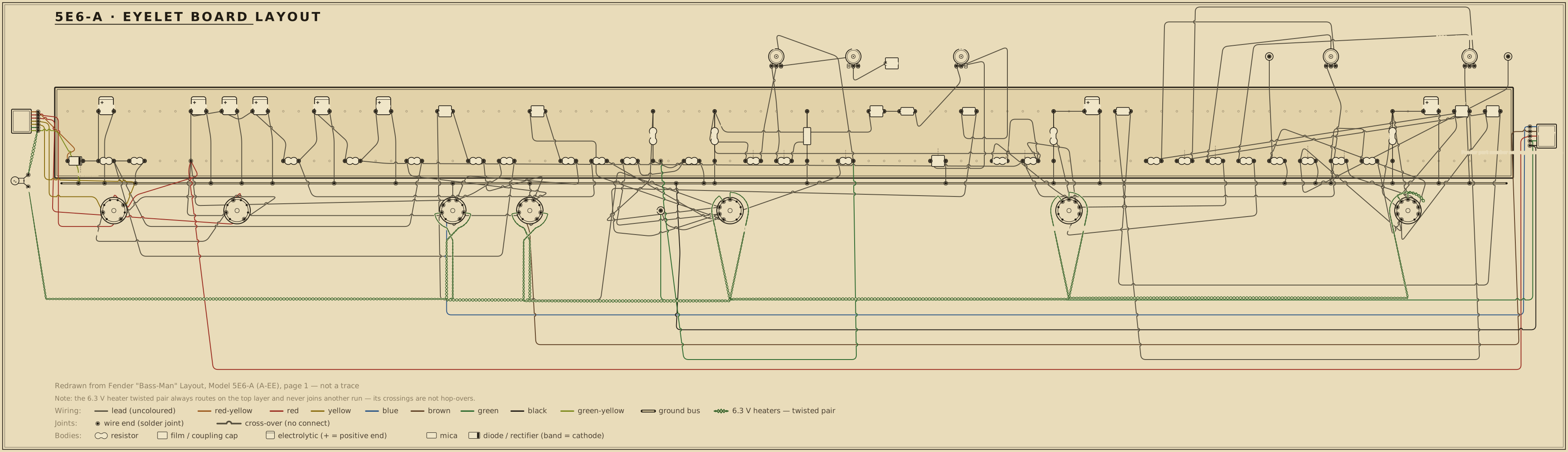
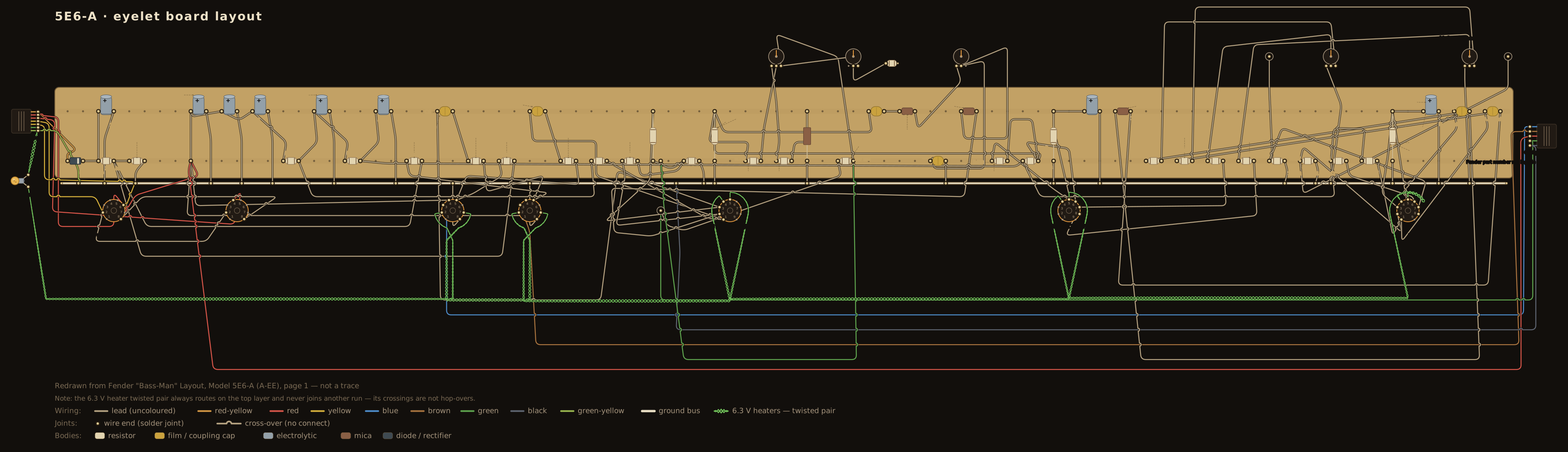
Board layout — redrawn reference diagram · source noted on the drawing Print sheet ↗
5E6-A eyelet board layout — an original diagram redrawn from the published layout drawing, showing the principal parts in the order that drawing places them on the board, drawn in the period layout-sheet style with each value lettered on the part.

Scroll the drawing sideways to read the whole board — the source line and the colour legend run along the bottom of the sheet — or open the full-size diagram in its own tab. Values are lettered on the parts in the period shorthand — .02-400, 250-5, 1MEG: how to read it.

Machine-checked wiring. Every modelled part the operating-point netlist places on this board has been verified in CI, terminal for terminal, to be electrically equivalent to the circuit's simulated netlist. This diagram documents connectivity and part arrangement — it is not a dimensioned 1:1 build template.

Details

The modelled parts are the tube sockets, the plate, cathode and grid-leak resistors, the power-rail droppers, and the coupling and bypass capacitors whose two leads are both named DC nodes; the check proves the same net structure, with no missing or extra connections. Parts outside that DC model — the volume / tone / mixer control-network internals, the negative-bias front end, and the heater chain, pilot lamp and power-transformer / rectifier AC side — are drawn from the cited sources but are not machine-checked; the CI report enumerates every one of their terminals so the boundary is explicit rather than silent.

Board and part positions are drawn at diagram scale, and lead dress, grounding paths, and physical spacing all matter in a high-voltage chassis. If you build from it, verify every connection against the schematic above and the operating-point table below as you go.

Operating point vs. published chart

Chart values read from the published drawing — or, where the drawing carries no voltage chart, from the cited published measurements (never reproduced). The simulated column is this circuit's own netlist solved in ngspice by the run that gates it; every deviation beside it is those two numbers compared, not a separately stated figure. Tolerances are this project's verification targets: tube-pin nodes carry the tolerance the cited source states, or ±20% — the era's printed convention — where it states none, and power rails are held to tighter internal targets.

Node Chart Simulated Deviation Tolerance Note
BP1 420 V 420.0 V 0.0% ±8% first-filter node — plates, screens and OT centre tap all land here directly (no choke); the drawing also reads 410/405 V at nearby points on this same node
BP2 335 V 361.5 V 7.9% ±8% PI supply node after the first 10 kΩ dropper
BP3 275 V 314.9 V 14.5% ±8% preamp supply node after the second 10 kΩ dropper
PAY1 130 V 160.9 V 23.8% ±20% V1 channel-A (bright) plate
PAY2 130 V 160.9 V 23.8% ±20% V1 channel-B (normal) plate
KAY 2 V 2.5 V 26.2% ±20% shared V1 cathode, 820 Ω
P2A 156.4 V V2 plate — not confidently isolated from the surrounding printed figures this pass; simulated value only
K2A 2.4 V V2 cathode, 1.5 kΩ — same caveat as P2A
PPI 295.2 V V3 (cathodyne) plate, 56 kΩ load — a printed figure near +210 V exists on the sheet but this pass could not confidently pin it to this node; simulated value only
KPI 68.1 V V3 cathode pin, above the 1.5k+56k split — same caveat as PPI
JPI 66.3 V 1.5k/56k cathode-split junction — the cathodyne grid's DC reference through the 1 MΩ leak; same caveat as PPI
G51 −42 V −42.0 V 0.0% ±8% 6L6G fixed bias via 220k from the bias supply; printed magnitude ~42 V, sign inferred negative (see meta.yaml sources)

Tube-pin nodes are checked at the tolerance the cited source states, or at the era's ±20% convention where it states none; power-rail nodes are held to tighter internal verification targets. Simulated figures are the netlist's DC solution, not measurements from a chassis.

The output stage behind these numbers can be drawn: the load line explorer plots this circuit's 6L6G pair at the DC operating point its netlist carries — 420 V on the plates with a −42 V grid bias — and marks where the load line crosses. This circuit is published as a draft, so that operating point is not verified against a published chart: the table and notes above say what each figure rests on.

Parts list

Every designator in this list appears on the schematic above, and every designator on the schematic appears here — the two are checked against each other in both directions, a valve's two halves counting as one bottle (V1A and V1B are both V1). Six parts the drawing carries as annotations rather than numbered symbols are listed here without designators, and stand outside that check. Two rectifier tubes (V6/V7) are documented but not DC-modeled — an ideal B+ source stands in for the rectifier+PT, the corpus-wide convention. The tone-stack ladder, the volume-pot bodies and the channel-jumper cap sit off the DC model's path too (DC-open or abstracted), even though each carries its own schematic designator.

RefPartValue / ratingRole
RG1 Carbon comp resistor 1 MΩ · ½ W Channel-A (bright) input grid leak
RG2 Carbon comp resistor 1 MΩ · ½ W Channel-B (normal) input grid leak
RL1 Carbon comp resistor 100 kΩ · ½ W V1A plate load
RL2 Carbon comp resistor 100 kΩ · ½ W V1B plate load
RK1 Carbon comp resistor 820 Ω · ½ W Shared 12AY7 (V1) cathode bias
C1 Electrolytic capacitor 250 µF · 6 V Shared V1 cathode bypass
CC1 Coupling capacitor 0.02 µF · 600 V V1A → channel-A padding resistor (DC-open)
CC2 Coupling capacitor 0.02 µF · 600 V V1B → channel-B padding resistor (DC-open)
CJ1 Mica capacitor 100 pF (printed .0001) Channel jumper, bridging channel-A's and channel-B's post-coupler nodes directly (DC-open). At low resolution it reads as one part with the RFB resistor above it; the two are unrelated
RP1 Carbon comp resistor 100 kΩ · ½ W Channel-A volume-pot padding resistor, coupler → VR1 hot lug
RP2 Carbon comp resistor 100 kΩ · ½ W Channel-B volume-pot padding resistor, coupler → VR2 hot lug
VR1 Audio-taper potentiometer 1 MΩ Channel-A (bright) volume
VR2 Audio-taper potentiometer 1 MΩ Channel-B (normal) volume
RM1 Carbon comp resistor 270 kΩ · ½ W Channel-A mixer into V2 grid (DC-open, wiper-fed)
RM2 Carbon comp resistor 270 kΩ · ½ W Channel-B mixer into V2 grid (DC-open, wiper-fed)
RL3 Carbon comp resistor 100 kΩ · ½ W V2 plate load
RK2 Carbon comp resistor 1.5 kΩ · ½ W V2 cathode bias
C2 Electrolytic capacitor 25 µF · 25 V V2 cathode bypass
RFB Carbon comp resistor 10 MΩ V2 plate-to-grid feedback/self-bias resistor, drawn as a loop above V2 on the A-EE sheet. Its left end lands on the post-mixer V2 grid node, not on the input jacks
VR5 Linear potentiometer 5 kΩ Presence — hot lug on the shared presence/NFB bus, wiper → CPR → ground
CPR Film capacitor 0.1 µF · 200 V Presence wiper → ground
RNF Carbon comp resistor 20 kΩ Negative feedback, speaker node → the presence/NFB bus (this family's usual take-off; cf. the 5F6's 27 kΩ)
RBL Carbon comp resistor 220 kΩ · ½ W Bleeder, V2 plate node → ground
RTS Carbon comp resistor 220 kΩ · ½ W V2 plate node → the bass-pot wiper junction
RBS Carbon comp resistor 220 kΩ · ½ W Bass shelf, wiper junction → CBS
CBS Mica capacitor 0.005 µF (printed .005) Bass shelf → ground. The sheet is dense here and the printed figure reads .005, not the .0005 the same patch of ink can suggest — a factor of ten
VR4 Audio-taper potentiometer 1 MΩ Bass — wiper on the shelf junction, hot lug on the presence/NFB bus
C3 Coupling capacitor 0.1 µF · 200 V V2 plate → C4 (first of two series caps into the treble network)
C4 Mica capacitor 250 pF (printed .00025) C3 → the treble network (second of two series caps)
VR3 Audio-taper potentiometer 1 MΩ Treble — wired as a rheostat (wiper strapped to its hot lug), the family's usual ladder trick
C7 Film capacitor 0.01 µF · 400 V Treble network → ground
C8 Mica capacitor 47 pF (printed 47 MMF) Treble network → V3 grid
RLA Carbon comp resistor 56 kΩ · ½ W V3 (cathodyne) plate load
RKA Carbon comp resistor 1.5 kΩ · ½ W V3 cathode-split resistor between the cathode pin KPI and the junction JPI (grid-leak return)
RKB Carbon comp resistor 56 kΩ · ½ W V3 cathode-split resistor between the junction JPI and ground
RGPI Carbon comp resistor 1 MΩ · ½ W V3 grid leak, returned to the cathode-split junction (through the tone network, DC-open)
C5 Coupling capacitor 0.1 µF · 400 V V3 plate → V4 grid
C6 Coupling capacitor 0.1 µF · 200 V V3 cathode → V5 grid
R5s Carbon comp resistor 1.5 kΩ · ½ W V4 grid stopper
R6s Carbon comp resistor 1.5 kΩ · ½ W V5 grid stopper
RGL1 Carbon comp resistor 220 kΩ · ½ W V4 grid leak, from the bias supply
RGL2 Carbon comp resistor 220 kΩ · ½ W V5 grid leak, from the bias supply
RD1 Power resistor 10 kΩ Rail dropper B+1 → B+2
RD2 Power resistor 10 kΩ Rail dropper B+2 → B+3
C9 Electrolytic capacitor 16 µF · 450 V Filter, B+1 (first of three cans at the same node — plates/screens/OT centre-tap area)
C10 Electrolytic capacitor 16 µF · 450 V Filter, B+1 (second of three cans)
C11 Electrolytic capacitor 16 µF · 450 V Filter, B+1 (third of three cans)
C12 Electrolytic capacitor 16 µF · 450 V Filter, B+2
C13 Electrolytic capacitor 8 µF · 450 V Filter, B+3
D1 Rectifier (bias) selenium (silicon diode in modern builds) Bias supply rectifier
RB1 Carbon comp resistor 3.3 kΩ · ½ W Bias supply series resistor (changed from a higher value between the 5E6 and 5E6-A revisions — see meta.yaml sources)
C14 Electrolytic capacitor 100 µF · 25 V Bias supply filter
RB2 Carbon comp resistor 56 kΩ · ½ W Bias supply bleeder
V1 Preamp tube 12AY7 Two-channel input (V1A/V1B)
V2 Preamp tube 12AY7 Second gain stage (one section wired)
V3 Preamp tube 12AX7 Self-biased split-load (cathodyne) phase inverter (one section wired)
V4 Power tube 6L6G Push-pull output (upper); simulated on the 5881 family model
V5 Power tube 6L6G Push-pull output (lower); simulated on the 5881 family model
V6 Rectifier tube 5U4GA Rectifier, tube 1 of 2 (parallel full-wave, not DC-modeled)
V7 Rectifier tube 5U4GA Rectifier, tube 2 of 2 (parallel full-wave, not DC-modeled)
Power transformer Fender part number not legible on this scan HT + heaters + rectifier filament
T3 Output transformer Fender part number not legible on this scan Push-pull output into four 10-inch speakers
Film capacitor 0.05 µF · 600 V (×2) AC-line bypass, ground switch / AC switch (annotation only)
Fuse 3 A AC line fuse
Switch SPST Ground switch (annotation only)
Switch SPST Standby switch (annotation only)
Lamp Pilot lamp Panel pilot light, off the 6.3 V heater winding

Circuit story

The mature narrow-panel revision of the 4x10 tweed Bassman's dual-rectifier era — the last stop before the 5F6 brought in the three-knob tone stack and the long-tailed-pair phase inverter that made the line famous. Where the 5F6 and 5F6-A each carry a single mercury-vapour or GZ34 rectifier feeding the amp through a choke, the 5E6-A still runs the older scheme its 5D6 ancestor established: two 5U4GA rectifier tubes in parallel and no choke at all, plates and screens landing straight on the first filter node.

Circuit walkthrough (short form)

Two channels (each: 1 MΩ grid leak, no stopper) → V1 12AY7 (100 kΩ plates, shared 820 Ω cathode with 250 µF bypass) → 0.02 µF couplers → 1 MΩ volume pots → 270 kΩ mixers → V2 12AY7, a single-section extra gain stage (100 kΩ plate, 1.5 kΩ/25 µF cathode) → Presence(5k)/Bass/Treble network → V3 12AX7, a single-section self-biased split-load (cathodyne) phase inverter: 56 kΩ plate, cathode split 1.5 kΩ (between the cathode pin and the grid-leak's return junction) + 56 kΩ (junction to ground) — the same shape as the 5F4's V3B — → 0.1 µF couplers + 1.5 kΩ stoppers → 6L6G pair, fixed-biased through 220 kΩ leaks, screens tied straight to the supply with no series resistor → output transformer into four 10-inch speakers.

Power: two 5U4GA rectifiers in parallel (no choke) → +420 V (plates, screens, OT centre tap — the drawing also reads +410/+405 V at nearby points on this same undropped node) → 10 kΩ → +335 V (V3 supply) → 10 kΩ → +275 V (V1/V2 supply). A selenium-rectifier bias supply (3,300 Ω, 100 µF, 56 kΩ bleeder) delivers roughly −42 V to the 6L6G grid leaks.

What makes this circuit distinct from its neighbors

  • No choke. Every other verified amp in this family (5F6, 5F6-A, 5F4) filters through the 14684 choke between the first reservoir cap and the screens. The 5E6-A drawing shows none: the plates, screens and OT centre tap all read within a few volts of each other at the same node, consistent with three separate 16 µF/450 V cans sitting at slightly different physical points on one low-impedance rail rather than three RC-filtered stages.
  • Two rectifier tubes, not one. The 5E6-A keeps the "dual rectifier" scheme this archive's Bassman family timeline describes for the 5D6 lineage: two 5U4GA tubes wired in parallel off separate secondary taps, both cathodes landing on the same first-filter node — extra current capacity for the 4x10 cab's fixed-bias 6L6G pair.
  • Cathodyne, not long-tailed-pair. The corpus's own existing citation chain already had this right — the family timeline's 5F6 entry reads "swapped the cathodyne splitter for a long-tailed-pair phase inverter" — the 5E6-A's V3 is a single 12AX7 section, self-biased with a split cathode resistor exactly the way the 5F4's V3B is (1.5 kΩ junction + 56 kΩ tail), just without the extra driver stage the 5F4 puts in front of it.
  • No cathode follower. That innovation is the 5F6's, not this circuit's: the signal runs V1 → V2 → tone network → V3 directly, with V2 doing the gain-recovery work a cathode follower would later take over.

The 5E6 → 5E6-A revision

The 5E6 and 5E6-A drawings share the same drawing code (A-EE) and are otherwise identical circuits. The one substantive difference is a handwritten note on the 5E6 sheet beside the bias-supply series resistor: "THIS CHANGE TO INCREASE BIAS ON PLATES SO WON'T GET HOT", with the original resistor value struck through and "3300" written in. The 5E6-A drawing prints 3,300 Ω cleanly with no annotation — the fix formalized. A smaller series resistor in this bias-supply topology (selenium rectifier → series R → filter cap → bleeder) delivers a larger-magnitude (more negative) bias voltage, which lowers 6L6G quiescent plate current and dissipation — exactly the fix the note describes. This is the one circuit-level change the "-A" suffix marks.

What the drawing resolves, and what it does not

The title block, tube complement (a dual-5U4GA rectifier and a 2×12AY7/1×12AX7 preamp split), the rail chain and V1's front end all read consistently off the drawing and agree across the two archived copies of the same A-EE sheet. They do not all agree with the printed chart, and this entry is published as a draft for that reason: four of the twelve nodes miss, and they miss as one fault rather than four. The preamp rail reads 315 V simulated against the chart's 275 V — 14.5% out, against the 8% this corpus holds a rail to — and the three nodes it feeds follow it up: both 12AY7 plates at 161 V against a printed 130 V (23.8%) and the shared 12AY7 cathode at 2.5 V against 2 V (26.2%), both past the chart's own ±20% convention. The two printed 10 kΩ droppers carry less current in the model than the drawing's own rail figures imply, so every node below the first dropper sits high; the likeliest reading error is which node feeds the 6L6G screens. The rails above that dropper, the output stage and its bias all gate clean. Three things the sheet does not resolve are flagged here rather than guessed at:

  • V2's own pin voltages — the printed figures around V2 sit in a cluster dense enough that they cannot be confidently separated from the neighbouring tone-network figures. The voltage table carries them as simulated-only, with no chart figure to check against.
  • V3's plate/cathode/junction pin voltages — a printed figure cluster near +210/+72/+1.7 V sits close to the 12AX7 on the sheet, but the obvious assignment (+72 V to the cathode pin, +1.7 V to the grid-leak junction) does not survive simulation: a 12AX7 cannot hold ~1.25 mA against the roughly −70 V grid-to-cathode bias that pairing implies, so at least one figure belongs to another node — possibly to V2. The netlist therefore uses the 5F4's V3B values verbatim (56k plate, 1.5k/56k cathode split, the same shape), and the voltage table leaves PPI/KPI/JPI informational rather than assign the printed numbers to pins the physics rules out.
  • One lug of the Presence/Bass/Treble ladder — the ladder is drawn as read (see below), with a single residual lug-level uncertainty annotated on the schematic itself. Because the network is entirely DC-open, none of it bears on the operating point; it does mean the tone-stack lab has no topology to plot for this amp, whose ladder is not one of the shapes it solves.

All three are draft-status gaps, not disputes: nothing here contradicts the drawing. The bias-supply figure's printed sign is also not clearly legible on the archived scan (magnitude ~42 V is clear); it is read as negative for consistency with every other fixed-bias amp in this corpus and because the circuit only functions as drawn (a fixed-bias output pair) with a negative supply.

The tone ladder, lug by lug

The schematic redraws the Presence/Bass/Treble ladder from a lug-level read of the A-EE sheet: a bleeder, a bass shelf, and a shared presence/NFB bus fed by a 20 kΩ resistor off the speaker node — the family's usual feedback take-off — with the treble pot wired as a rheostat, the same trick the family's three-knob ladders use for their bass pot.

Two details of that region are easy to misread and are worth stating plainly. What looks at low resolution like one "10 MΩ channel-linking resistor in series with a small mica cap" is two unrelated parts: RFB, a light V2 plate-to-grid feedback resistor drawn as a loop above V2, whose left end lands on the post-mixer V2 grid node rather than on the input jacks; and CJ1, a channel-jumper cap bridging the two channels' post-coupler nodes directly. Each channel also carries a 100 kΩ padding resistor from its coupler to its volume-pot hot lug (RP1/RP2). And the bass-shelf mica reads .005, i.e. 0.005 µF (CBS), not the .0005 the same dense patch of ink can suggest — a factor of ten, and worth a third read before this entry leaves draft.

One residual uncertainty, flagged rather than guessed past: which of the bass pot's two end lugs is the "hot" one riding the shared presence/NFB bus and which is the "cold" one feeding the fixed shelf network. It is drawn as read, the two lugs sit close together on the sheet, and the schematic carries a comment saying so right above that block. A lug-by-lug re-check would firm it up before this entry leaves draft.

The board

The board diagram is redrawn from the A-EE sheet's own layout page: the principal components in the order the drawing shows them, with their hookup. The parallel-rectifier supply is the feature of it — two 5U4GAs and no choke, so plates, screens and the output transformer's centre tap all land on one first-filter node carrying three 16 µF cans, where most of this corpus's tweed amps split the screen supply behind a choke.

The drawn point-to-point wiring is proved electrically equivalent to the simulated circuit within the documented DC scope, every valve anchored, with the two rectifiers outside the DC model by the same convention every other rectifier here follows. The five panel pots sit off the board as the sheet draws them, and the primary leads land on chassis switches; the fixed tone-network parts are on the board.

Lineage

The Bassman family history records the 5F6/5F6-A's long-tailed-pair phase inverter as a revision of "the cathodyne splitter" that came before it. This circuit is that predecessor: the corpus carries the edge in both directions, 5E6-A → 5F6. Behind the 5E6-A stand the plain 5E6 and the 5D6, neither of them a documented circuit here, so this entry claims no ancestor of its own.

Sources