Fender's smallest amp gains a trem foot. The Vibro Champ is the AA764 drawing
family's tremolo-equipped sibling: the same five-watt, single-12AX7-preamp,
single-ended-6V6 recipe as the plain Champ, plus a second,
dedicated 12AX7 running a tremolo whose output lands on the second preamp
stage's cathode. Fender's own drawing prints "VIBRO-CHAMP AA764" — the
identical designation the non-tremolo Champ sheet carries — so this circuit
is filed under the qualified id aa764-vibro, leaving the plain Champ's
aa764 to the drawing that carries no tremolo. Two print runs of the
drawing exist (an earlier "Fender
Electric Instrument Company" letterhead and a later CBS-era "A Division of
Columbia Broadcasting System" one); both carry the AA764 designation and the
same component values, and the earlier printing is the one cited here.
Signal path
Identical to the Champ, component-for-component. Two input jacks (high and
low) each sit behind a 68 kΩ grid stopper and share a 1 MΩ leak to
ground. From there:
V1A — 12AX7, 100 kΩ plate load, 1.5 kΩ cathode with a 25 µF
bypass. Its plate feeds the tone stack directly; both stack legs start with a
capacitor, so no DC reaches the controls.
Tone stack — the blackface treble-bass network. A 250 pF cap carries
the top end onto the 250 kΩ Treble control; a 100 kΩ slope resistor
feeds a 0.1 µF cap into the junction below the treble pot and a
0.047 µF cap into the 250 kΩ Bass control's lower leg, which returns
to ground through 15 kΩ. The treble wiper hands the recovered signal to a
1 MΩ Volume control.
V1B — 12AX7, 100 kΩ plate load. Its cathode resistor is 1.5 kΩ
with a 25 µF bypass, but it does not land on ground: it sits on a
47 Ω leg, and the 2.7 kΩ negative-feedback resistor from the speaker
jack lands on that same junction. The tremolo's Intensity control lands on
the cathode itself (see Tremolo below).
Output — a 0.02 µF coupling cap into the 6V6GT grid, held down by
a 220 kΩ leak. The 6V6 is cathode-biased on 470 Ω · 1 W with a
25 µF bypass, its screen wired straight to the second filter node with no
stopper, and its plate working into the 125A35A single-ended output
transformer — the same transformer aa764 uses.
Tremolo
A dedicated second 12AX7 bottle (both sections) — unlike the shared-
tube trem in 6G3, where the oscillator is the second half of the
driver tube, this is its own socket, the same arrangement the
Deluxe Reverb uses for its trem oscillator.
First section (pins 1–3) — an RC phase-shift oscillator. Its plate load
is 470 kΩ off the +340 V node between the two droppers, printing
+170 V; the cathode sits on 4.7 kΩ bypassed by 25 µF, printing
+1.6 V. A three-section ladder runs from the plate back to the grid:
0.02 µF to a Speed node, which the 3 MΩ reverse-audio Speed control
(a rheostat, with 100 kΩ in series on the pot) returns to ground;
0.01 µF to a second node, which a 1 MΩ returns to the cathode; and
0.01 µF to the grid, which a 1 MΩ returns to ground. The Vibrato
Pedal jack hangs on the ladder's middle node, so the pedal's footswitch
grounds that node and stops the oscillation.
Second section (pins 6–8) — a cathode follower, its grid taken straight
off the oscillator's plate and its plate tied directly to the +340 V node
with no plate load. Its cathode prints +175 V and feeds the wiper of the
25 kΩ reverse-audio Intensity control through 68 kΩ. One end of that
pot is grounded; the other goes straight to V1B's cathode, with no
capacitor anywhere in the path.
So this tremolo works on the preamp, not the output stage: the follower
pushes its oscillating current into V1B's cathode, moving that stage's bias
and with it its gain, and the Intensity control sets how much of that
current reaches the cathode rather than ground. The 6V6 is not touched by
it.
Power
315-0-315 V from the 125P1B power transformer — the same part number
the Champ's 320-0-320 V winding prints; the two AA764-family drawings simply
print their own figures for the identical transformer, a habit of the era's
Fender sheets that the Princeton family's drawings repeat — →
5Y3GT full-wave rectifier → three 20 µF · 450 V filter cans. The
chain reads +355 V at the reservoir (which also feeds the output
transformer primary), +340 V after a 1 kΩ · 1 W dropper at the 6V6
screen, and +320 V after a 10 kΩ · 1 W dropper at both 12AX7 plate
loads — the same dropper values the Champ uses, each rail printing a few volts
lower here, plausibly the tremolo oscillator's added current draw. A 1 A
slow-blow fuse and an AC switch sit ahead of the primary.
The heater circuit, read off the Vibro-Champ's own sheet
The Champ AA764 layout sheet exists only as a 2171 px copy that does not
resolve the socket pins, so the Champ's heater layer stays marked as unread.
The Vibro-Champ's page of the same drawing family was found at 6480 × 4058
(708 ppi), and its heater circuit is read from that: one green transformer lead
meets the red-yellow HT centre tap at a solder point and goes to a ground
arrow; the other green runs up to the pilot light, whose far terminal goes to a
ground triangle and whose fed terminal carries the arrow "to all 6.3V.
heaters". At both 12AX7 sockets — the preamp bottle and the tremolo bottle
alike — a short bow outside the socket rim ties pins 4 and 5 together and pin 9
carries a lead to a ground triangle, the 6.3 V parallel arrangement; at the
6V6GT pin 7 takes the lead to a ground triangle and heater pin 2 is a bare
terminal, the fed leg the arrow stands in for. Each socket's circle was fitted
to its drawn rim and the pins measured rather than read by eye; the 4–5 bows
are the only ink that leaves either pin. A single-ended supply, then, each
socket returning to chassis on its own, as the board has always drawn it — its
heater leads are now styled as heater wiring and the circuit is declared and
checked.
Excluded from the DC model: the tremolo oscillator
The tremolo oscillator (V4, both sections) is a running phase-shift
oscillator — it has no static quiescent point, the same category of
exclusion as the Deluxe Reverb's V5. Its printed chart pins (+170 V / +1.6 V
first section, +340 V / +175 V second section) are read directly off the
sheet and recorded on this page, but are not modelled or gated: the
simulated deck omits V4 entirely.
Both of its sections draw from the +340 V node (BP2), between the two
droppers: the oscillator through its 470 kΩ plate load, the follower's plate
directly. Leaving the bottle out therefore means BP2, and the +320 V rail
below it, carry about 2.9 mA less in this model than the real circuit did,
which is why both rails read a few volts above the chart (see below).
The follower's cathode is also DC-coupled into V1B's cathode through 68 kΩ
and the Intensity control, and how much of its roughly 2.5 mA lands there
depends on the control's setting, which the drawing does not state. Holding
the follower at its printed +175 V and moving the wiper from the grounded end
to the V1B end takes V1B's cathode from 1.65 V to 3.87 V and its plate from
213 V to 323 V. The printed +1.5 V and +200 V describe one setting of a knob
the sheet does not record, so V1B's cathode and plate are reported here for
reference rather than gated.
Reading against the printed chart
The drawing prints a full voltage chart, every value set at ±20 %, read to
ground with an electronic voltmeter. Driving the reservoir at its printed
+355 V and solving everything below it:
| Node |
Chart |
Simulated |
Deviation |
| Screen rail (BP2) |
+340 V |
+349.1 V |
2.7 % |
| Preamp rail (BP3) |
+320 V |
+326.9 V |
2.2 % |
| V1A plate / cathode |
+205 V / +1.6 V |
+215.0 V / +1.7 V |
4.9 % / 4.9 % |
| 6V6 cathode (K2) |
+21 V |
+22.2 V |
5.9 % |
| V1B plate / cathode |
+200 V / +1.5 V |
+216.6 V / +1.7 V |
for reference — see above |
Every gated node lands inside the drawing's own ±20 % convention; the worst
is the 6V6 cathode at 5.9 %. The drawing prints +21 V beside the 6V6's
cathode, pin 8, on both the schematic and the layout page; its grid carries
no figure. V1B's two figures are simulated with the tremolo left out; the
range its injection spans is given above.
One value on the chart is deliberately not simulated. The drawing prints
+355 V at the reservoir and +342 V at the 6V6 plate; the gap between
them is the output transformer primary's winding resistance, which the
drawing does not publish — the same convention the Champ entry documents for
the same 125A35A part.
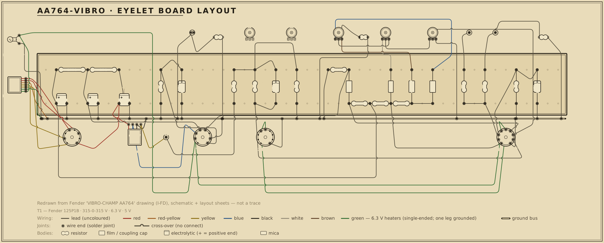
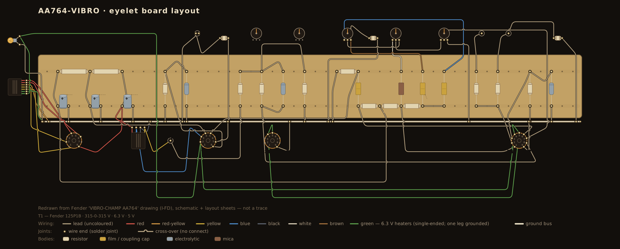
The tremolo block, as drawn
The schematic on this page draws the tremolo as the factory sheet does: the
oscillator on V4's pins 1–3 with its three-section ladder, the follower on
pins 6–8, the 68 kΩ into the Intensity wiper, and the pot's far end
labelled onto V1B's cathode. The factory layout page mounts the ladder, the
oscillator's cathode network, both 1 MΩs and the follower's 68 kΩ on the
eyelet board between the 6V6's cathode network and the feedback divider, the
470 kΩ plate load across V4's own socket, and the Speed control's 100 kΩ on
its pot. The board drawing on this page draws all of that except the 470 kΩ,
with the ladder's single factory column folded over the two eyelet rows and
the audio path from the feedback divider rightward shifted five columns to
make room; it otherwise reuses the
Champ's arrangement verbatim, since the two circuits' audio paths are
component-for-component identical (see above). The drawn wiring is proved
electrically equivalent to the simulated circuit, with V4 excluded from that
check just as it is excluded from the deck.