5C1 Wide‑panel Champ‑style · 1953–1955 · 4 W

✓ verified 2026-08-08
Schematic — redrawn in KiCad · scroll to zoom, drag to pan
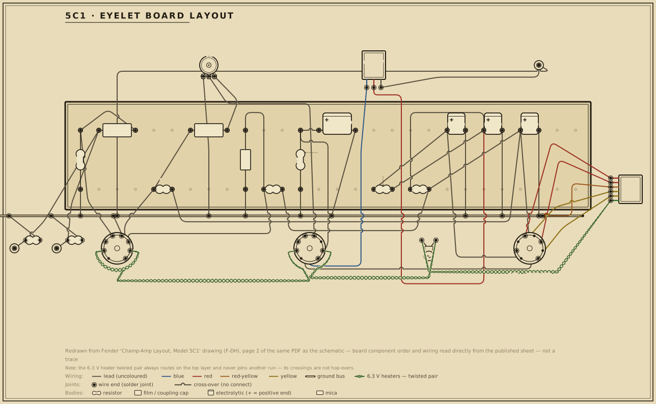
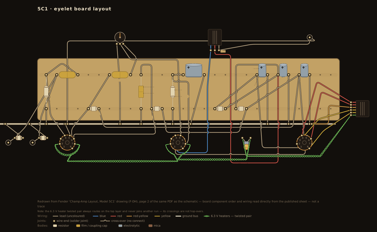
Board layout — redrawn reference diagram · source noted on the drawing Print sheet ↗
5C1 eyelet board layout — an original diagram redrawn from the published layout drawing, showing the principal parts in the order that drawing places them on the board, drawn in the period layout-sheet style with each value lettered on the part.

Scroll the drawing sideways to read the whole board — the source line and the colour legend run along the bottom of the sheet — or open the full-size diagram in its own tab. Values are lettered on the parts in the period shorthand — .02-400, 250-5, 1MEG: how to read it.

Machine-checked wiring. Every modelled part the operating-point netlist places on this board has been verified in CI, terminal for terminal, to be electrically equivalent to the simulated netlist this circuit is verified against. This diagram documents connectivity and part arrangement — it is not a dimensioned 1:1 build template.

Details

The modelled parts are the tube sockets, the plate, cathode and grid-leak resistors, the power-rail droppers, and the coupling and bypass capacitors whose two leads are both named DC nodes; the check proves the same net structure, with no missing or extra connections. Parts outside that DC model — the volume / tone / mixer control-network internals, the negative-bias front end, and the heater chain, pilot lamp and power-transformer / rectifier AC side — are drawn from the cited sources but are not machine-checked; the CI report enumerates every one of their terminals so the boundary is explicit rather than silent.

Board and part positions are drawn at diagram scale, and lead dress, grounding paths, and physical spacing all matter in a high-voltage chassis. If you build from it, verify every connection against the schematic above and the operating-point table below as you go.

Operating point vs. published chart

Chart values read from the published drawing — or, where the drawing carries no voltage chart, from the cited published measurements (never reproduced). The simulated column is this circuit's own netlist solved in ngspice by the run that gates it; every deviation beside it is those two numbers compared, not a separately stated figure. Tolerances are this project's verification targets: tube-pin nodes carry the tolerance the cited source states, or ±20% — the era's printed convention — where it states none, and power rails are held to tighter internal targets. Every gated node lands within target — worst deviation 9.7%.

Node Chart Simulated Deviation Tolerance Note
BP2 320 V 324.4 V 1.4% ±20% 6V6 plate (via OT primary, DCR omitted) — single 500 Ω resistor dropper off the reservoir, no choke on this pre-5E1 circuit
BP3 260 V 249.8 V 3.9% ±20% shared rail after the 25 kΩ dropper off BP2 — feeds the 6V6 screen (drawn off the far side of the 25 kΩ from its own plate, not off BP2) and the whole 6SJ7 plate/screen circuit
P1 149.3 V 6SJ7 plate — chart reads +130 V, but this stage's grid-leak (contact) bias has no DC current path in the project's grid-current-free Koren tube models (models/METHODOLOGY.md, v0 limitation): with only a capacitor and a 5 Meg leak at the grid, this deck settles Vg1 at 0 V rather than the real tube's small negative contact bias, so the simulated plate current — and this node — is not comparable to the chart. Reported for reference, not gated.
K2 14 V 15.4 V 9.7% ±20% 6V6GT cathode, chart pin value (500 Ω, 25 µF bypass)

Tube-pin nodes are checked at the tolerance the cited source states, or at the era's ±20% convention where it states none; power-rail nodes are held to tighter internal verification targets. Simulated figures are the netlist's DC solution, not measurements from a chassis.

The output stage behind these numbers can be drawn: the load line explorer plots this circuit's 6V6GT at the DC operating point its netlist carries — 324 V on the plates with a 500 Ω cathode resistor — and marks where the load line crosses.

Parts list

Every designator in this list appears on the schematic above, and every designator on the schematic appears here — the two are checked against each other in both directions, a valve's two halves counting as one bottle (V1A and V1B are both V1). Three parts the drawing carries as annotations rather than numbered symbols are listed here without designators, and stand outside that check. Numbering follows the schematic. The AC-line section (power transformer, fuse, line cap) is drawn as annotation only and carries no designator. Values are from the published Champ 5C1 (F-DH) drawing.

RefPartValue / ratingRole
R1 Carbon comp resistor 75 kΩ · ½ W Input 1 to ground
R2 Carbon comp resistor 75 kΩ · ½ W Input 2 to ground
R3 Carbon comp resistor 5 MΩ · ½ W 6SJ7 grid leak (contact bias — no cathode resistor)
R4 Carbon comp resistor 2 MΩ · ½ W 6SJ7 screen dropper
R5 Carbon comp resistor 250 kΩ · ½ W 6SJ7 plate load
R6 Wirewound resistor 500 Ω · 2 W 6V6 cathode bias
R7 Power resistor 500 Ω · 1 W Rail dropper B+1→B+2
R8 Power resistor 25 kΩ · 1 W Rail dropper B+2→B+3
VR1 Audio-taper potentiometer 1 MΩ Volume
C1 Coupling capacitor 0.02 µF · 600 V Input → 6SJ7 grid
C2 Bypass capacitor 0.05 µF · 600 V 6SJ7 screen bypass
C3 Coupling capacitor 0.02 µF · 600 V 6SJ7 plate → volume pot
C4 Electrolytic capacitor 25 µF · 25 V 6V6 cathode bypass
C5 Electrolytic capacitor 8 µF · 450 V Filter, B+1 (reservoir)
C6 Electrolytic capacitor 8 µF · 450 V Filter, B+2
C7 Electrolytic capacitor 8 µF · 450 V Filter, B+3
V1 Preamp tube 6SJ7 Single gain stage
V2 Power tube 6V6GT Single-ended output
V3 Rectifier tube 5Y3GT Full-wave rectifier (V3A/V3B)
T1 Output transformer ≈5 kΩ : 8 Ω Single-ended output (impedance not marked on the drawing; typical SE 6V6 load)
Power transformer HT · 6.3 V · 5 V HT secondary (voltage not marked; +340 V reservoir implies ≈345-0-345) + heater and rectifier windings
Line capacitor 0.05 µF · 600 V Across the AC line at the fuse
Fuse 2 A AC-line fuse

Circuit story

The earliest circuit-numbered Champ, and the corpus's first octal-preamp circuit: a single 6SJ7 sharp-cutoff pentode giving one stage of voltage gain, one 1 MΩ volume control, a cathode-biased 6V6 single-ended output, and a 5Y3GT rectifier — no tone control and no phase inverter. Wide-panel tweed cabinet, produced circa 1953–1955. It carries the Champion 600's circuit forward under Fender's new "Champ" model name (history/families/champ.yaml) and is the direct topological ancestor of the 12AX7-based 5E1 that replaces it: the wide-panel-to-narrow-panel revision (5D1) that sits between the two is a short-lived component revision of this same circuit, not a documented redesign of its own (no landed circuit page).

Circuit walkthrough (short form)

Two input jacks, each shunted to ground by its own 75 kΩ resistor, sum into a single 0.02 µF coupling cap → V1 (6SJ7 pentode, grid-leak/contact biased: a 5 MΩ leak returns the grid to ground and the cathode grounds directly, with no cathode resistor at all — the plate carries a 250 kΩ load, the screen a 2 MΩ dropper bypassed by 0.05 µF) → 0.02 µF coupling → 1 MΩ volume pot → V2 6V6GT (cathode-biased, 500 Ω with 25 µF bypass, grid returned to ground through the volume pot) → single-ended output transformer (≈5 kΩ : 8 Ω, typical for a single-ended 6V6; the drawing doesn't mark it) → speaker. No negative feedback loop on this circuit (the 5E1 does not add one either; NFB into the Champ line waits for the 5F1).

Power: a center-tapped HT winding feeds the 5Y3GT full-wave rectifier into a reservoir at +340 V. Unlike every later Champ in the line, there is no choke here — a plain 500 Ω resistor drops the rail to +320 V, which supplies only the 6V6 plate (through the output-transformer primary); a 25 kΩ resistor then drops that node further to +260 V, and it is this third rail — not the plate's own +320 V node — that the drawing routes to the 6V6 screen, alongside the whole 6SJ7 plate/screen circuit. So the single output tube's screen shares a dropper-filtered rail with the preamp rather than riding its own plate's node, which is the opposite of where a reader would guess it sits at a glance. Three 8 µF / 450 V cans do the filtering — the same three-can arrangement the 5E1 keeps, just filtered through resistors instead of the choke the 5E1 introduces.

The 6SJ7, and why it has no cathode resistor

The 5C1's preamp tube is an octal metal pentode, not the 9-pin 12AX7 twin triode every later Champ in the line uses — grid No.1 comes out on a base pin rather than a top cap, which is what let Fender mount it flat on a chassis-board like everything else (reference/tubes/6sj7.yaml). Fender bias this stage the cheapest way available: grid-leak (contact) bias. The cathode ties straight to ground, and a single 5 MΩ resistor returns the grid to ground too — with no cathode resistor anywhere in the stage. A real 6SJ7 run this way self-biases to a small negative grid voltage from grid contact potential and rectified grid current, not from a cathode voltage drop. It is a real, period-correct circuit (matched by the printed chart's own +130 V plate reading, well below what a zero-bias 6SJ7 would show), and it disappears from the Champ line entirely once the 5E1's 12AX7 arrives with conventional cathode-biased stages.

A documented model limitation, not a circuit claim

The project's tube models are fitted from datasheet anchor points in the Koren model form and explicitly carry no grid-current path (models/METHODOLOGY.md, "No grid-current model (v0)" — confirmed in models/6sj7.inc's subcircuit, which ties the grid node only to the plate/cathode through AC-only Miller capacitances). Contact bias is exactly the mechanism that gap can't reach: with nothing but a capacitor and a to-ground resistor at the grid, this DC deck has no current path that would pull the grid negative, so it settles Vg1 at 0 V — a real (if small) departure from the tube's actual operating point. The 6SJ7 plate node is therefore marked chart: null in voltages.yaml (reported, never gated) rather than compared against the printed +130 V, which is honest about what the simulation can and cannot show here rather than papering over it with a misleading percentage. The B+ rails and the 6V6 stage — which do not depend on this mechanism — are fully chart-gated as usual.

Verification

The layout sheet prints a voltage chart (Fender's usual "read to ground with an electronic voltmeter, ±20%") giving the two B+ rails downstream of the reservoir (+320 V at the 6V6 plate, +260 V at the shared 6V6-screen/6SJ7 rail), the 6SJ7 plate (+130 V, not chart-gated — see above), and the 6V6 cathode (+14 V). pipeline/verify_amps.py simulates within tolerance on every chart-gated node: the 6V6 plate rail 1.4% off (+324.4 V), the shared screen/preamp rail 3.9% off (+249.8 V), and the 6V6 cathode 9.7% off (+15.4 V) — all inside Fender's own ±20% convention.

The screen node is where this circuit punishes a careless reading. Tie the 6V6 screen to the plate's own +320 V rail instead of the +260 V node the drawing actually feeds it from and the tube draws hard enough to pull the simulated cathode to +20.4 V — a 46% miss — while dragging the shared rail down to +303 V against its printed +260 V, a 17% miss on a node the tube is not supposed to load that hard. The chart catches it immediately, which is the point of gating against it.

The board, as the factory drew it

A genuine factory layout page exists for this circuit — page 2 of the same F-DH sheet — so the board order and the point-to-point wiring here are read from it rather than derived. It runs 6SJ7 preamp stage, 6V6GT output, resistor-dropped B+ chain, 5Y3GT rectifier, left to right: the reverse of the rectifier-first reading order every later Champ in this corpus uses.

The drawn wiring is proved electrically equivalent to the simulated netlist, so this board carries a verified wiring claim, and both drawing styles render with zero collision-lint findings and no waiver. One detail is worth naming because it is easy to get wrong on a circuit this small: the coupler out of the 6SJ7's plate feeds the volume pot, not the 6V6 grid directly, so a model that bridges plate to grid short-circuits past the control the drawing routes it through. It makes no difference to any simulated voltage — SPICE treats a coupling cap as open at DC either way — and every difference to whether the equivalence proof means anything.

Sources