AC30 Vox AC30/6‑style · 1961–1965 · 30 W

draft
Schematic — redrawn in KiCad · scroll to zoom, drag to pan
Board layout — redrawn reference diagram · source noted on the drawing Print sheet ↗
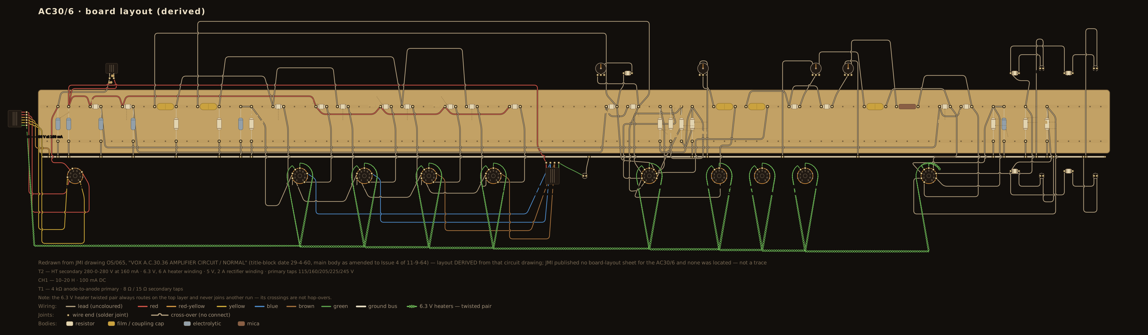
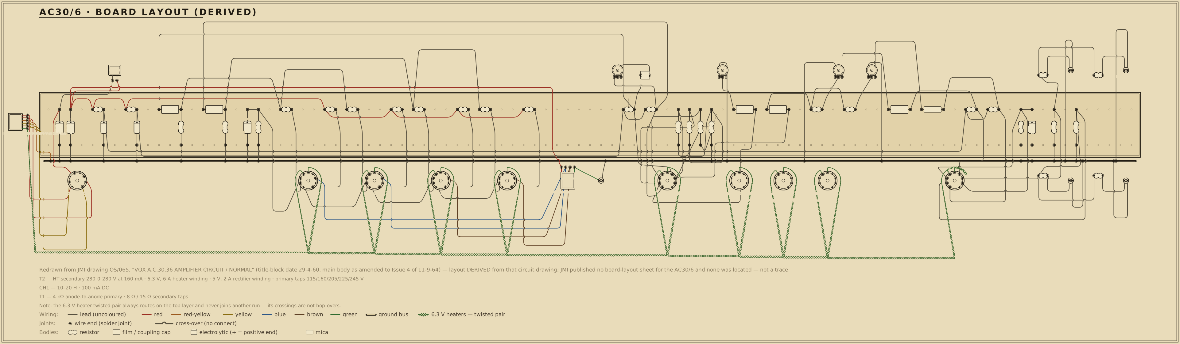
AC30 board layout — an original diagram reconstructed from the redrawn schematic (no factory layout sheet exists), showing the principal parts in board order, drawn in the period layout-sheet style with each value lettered on the part.

Scroll the drawing sideways to read the whole board — the source line and the colour legend run along the bottom of the sheet — or open the full-size diagram in its own tab. Values are lettered on the parts in the period shorthand — .02-400, 250-5, 1MEG: how to read it.

Machine-checked wiring. Every modelled part the operating-point netlist places on this board has been verified in CI, terminal for terminal, to be electrically equivalent to the circuit's simulated netlist. This diagram documents connectivity and part arrangement — it is not a dimensioned 1:1 build template.

Details

The modelled parts are the tube sockets, the plate, cathode and grid-leak resistors, the power-rail droppers, and the coupling and bypass capacitors whose two leads are both named DC nodes; the check proves the same net structure, with no missing or extra connections. Parts outside that DC model — the volume / tone / mixer control-network internals, the negative-bias front end, and the heater chain, pilot lamp and power-transformer / rectifier AC side — are drawn from the cited sources but are not machine-checked; the CI report enumerates every one of their terminals so the boundary is explicit rather than silent.

Board and part positions are drawn at diagram scale, and lead dress, grounding paths, and physical spacing all matter in a high-voltage chassis. If you build from it, verify every connection against the schematic above and the operating-point table below as you go.

Operating point vs. published chart

Chart values read from the published drawing — or, where the drawing carries no voltage chart, from the cited published measurements (never reproduced). The simulated column is this circuit's own netlist solved in ngspice by the run that gates it; every deviation beside it is those two numbers compared, not a separately stated figure. Tolerances are this project's verification targets: tube-pin nodes carry the tolerance the cited source states, or ±20% — the era's printed convention — where it states none, and power rails are held to tighter internal targets.

Node Chart Simulated Deviation Tolerance Note
BPN 290 V 295.3 V 1.8% ±20% front-end anode supply, after the 22 kΩ dropper R10 from the +320 V rail (8 µF C4). Simulated slightly high by construction: any current the excluded Vibrato/Tremolo chain draws from this side of the supply is not modelled
PV1A 170 V 172.1 V 1.2% ±20% V1 Brilliant-channel anode (pin 1), 220 kΩ load R5
PV1B 170 V 172.1 V 1.2% ±20% V1 Normal-channel anode (pin 6), 220 kΩ load R6 — the drawing prints the same figure at both anodes
KV1 1.6 V 1.7 V 5.1% ±20% V1's SHARED cathode (pins 3 and 8 tied), 1.5 kΩ R4 with a 25 µF bypass — one bias network for both channels' first stages, which is why neither half can be solved alone
BPPI 291.6 V phase-inverter supply node, after its own 22 kΩ dropper R11 from the +320 V rail (8 µF C8) — the drawing annotates the anodes, not this node
PPIA 230 V 227.1 V 1.2% ±20% phase-inverter anode, Brilliant/Normal side (100 kΩ load R18). Annotation revised from 285 V at ISS.3, 11-10-63
PPIB 230 V 227.1 V 1.2% ±20% phase-inverter anode, Vibrato/Tremolo side (100 kΩ load R19) — the drawing prints one figure for the pair. R19's multiplier glyph is the one value on this copy that does not resolve cleanly; see notes.md
KPI 62.2 V phase-inverter shared cathode, above the 1.2 kΩ R16
JPI 55 V 60.6 V 10.2% ±20% tail junction over the 47 kΩ R15 — the return for both 1 MΩ grid leaks, and the drawing's one annotated figure inside the inverter's cathode circuit
NGA 0.0 V EL84 grid-drive line, side A (V3 + V5), returned to ground through R20 220 kΩ — 0 V by construction
NGB 0.0 V EL84 grid-drive line, side B (V4 + V6), returned to ground through R21 280 kΩ — the drawing's asymmetric partner to R20
S3 319.5 V EL84 screen grid (V3), through its 100 Ω stopper R25 from the rail
S4 319.5 V EL84 screen grid (V4), through its 100 Ω stopper R26
S5 319.5 V EL84 screen grid (V5), through its 100 Ω stopper R29
S6 319.5 V EL84 screen grid (V6), through its 100 Ω stopper R30
KOUT 10 V 10.6 V 6.3% ±20% shared EL84 cathode over the single 50 Ω R24 (250 µF bypass) — the amp's entire bias arrangement for four valves. The drawing's 'QUIESCENT 10v' works out at 200 mA of cathode current for the quad, 50 mA a valve

Tube-pin nodes are checked at the tolerance the cited source states, or at the era's ±20% convention where it states none; power-rail nodes are held to tighter internal verification targets. Simulated figures are the netlist's DC solution, not measurements from a chassis.

The output stage behind these numbers can be drawn: the load line explorer plots this circuit's EL84 quartet at the DC operating point its netlist carries — 320 V on the plates with a 50 Ω cathode resistor — and marks where the load line crosses. This circuit is published as a draft, so that operating point is not verified against a published chart: the table and notes above say what each figure rests on.

Parts list

Every designator in this list appears on the schematic above, and every designator on the schematic appears here — the two are checked against each other in both directions, a valve's two halves counting as one bottle (V1A and V1B are both V1). Nine parts the drawing carries as annotations rather than numbered symbols are listed here without designators, and stand outside that check. Coupling and cathode-bypass capacitor VALUES are open at DC and do not enter the operating-point netlist; they are listed for completeness. Parts belonging to the Vibrato/Tremolo channel are marked — that channel is outside the DC netlist's scope (see notes.md), so its values are read from the drawing but not simulated, and the parts whose interconnection the published scan does not resolve carry no designator. The blue negative-feedback loop drawn across this copy is a later hand addition by a previous owner and is not a part of this circuit. Two capacitor values on the sheet were silently modernised between issues — the 1961/62 printing specifies 0.05 and 0.005 µF where later sheets, this one included, print 0.047 and 0.0047 µF for the same parts; the values recorded here are the ones OS/065 letters.

RefPartValue / ratingRole
J1 Jack socket 1/4 in Brilliant channel input 2
J2 Jack socket 1/4 in Brilliant channel input 1
R1 Carbon comp resistor 68 kΩ Brilliant channel input grid stopper (J1)
R2 Carbon comp resistor 68 kΩ Brilliant channel input grid stopper (J2)
R3 Carbon comp resistor 1 MΩ Brilliant channel input grid leak
J3 Jack socket 1/4 in Normal channel input 2
J4 Jack socket 1/4 in Normal channel input 1
R12 Carbon comp resistor 68 kΩ Normal channel input grid stopper (J3)
R13 Carbon comp resistor 68 kΩ Normal channel input grid stopper (J4)
R14 Carbon comp resistor 1 MΩ Normal channel input grid leak
J5 Jack socket 1/4 in Vibrato/Tremolo channel input 2
J6 Jack socket 1/4 in Vibrato/Tremolo channel input 1
R10 Power resistor 22 kΩ Rail dropper, +320 V → front-end anode supply (printed +290 V)
C4 Electrolytic capacitor 8 µF Front-end anode supply smoothing
R5 Carbon comp resistor 220 kΩ V1 anode load, Brilliant side (pin 1)
R6 Carbon comp resistor 220 kΩ V1 anode load, Normal side (pin 6)
R4 Carbon comp resistor 1.5 kΩ SHARED V1 cathode bias resistor — one network for both channels' first stages (pins 3 and 8 tied)
C1 Electrolytic capacitor 25 µF · 25 V V1 shared cathode bypass
C3 Mica capacitor 500 pF V1 Brilliant anode → Brilliant volume — the small coupler that gives the channel its name
C2 Coupling capacitor 0.047 µF V1 Normal anode → Normal volume
VR2 Log potentiometer 500 kΩ Brilliant channel volume
VR1 Log potentiometer 500 kΩ Normal channel volume
R9 Carbon comp resistor 220 kΩ Brilliant volume wiper → phase-inverter mixing node
R7 Carbon comp resistor 220 kΩ Normal volume wiper → phase-inverter mixing node
C5 Coupling capacitor 0.047 µF Mixing node → phase-inverter grid, side A
R11 Power resistor 22 kΩ Rail dropper, +320 V → phase-inverter supply
C8 Electrolytic capacitor 8 µF Phase-inverter supply smoothing
R18 Carbon comp resistor 100 kΩ Phase-inverter anode load, side A (Brilliant + Normal)
R19 Carbon comp resistor 100 kΩ Phase-inverter anode load, side B (Vibrato/Tremolo) — the one value whose multiplier glyph this copy leaves ambiguous; see notes.md
R8 Carbon comp resistor 1 MΩ Phase-inverter grid leak, side A, returned to the tail junction
R17 Carbon comp resistor 1 MΩ Phase-inverter grid leak, side B, returned to the tail junction
R16 Carbon comp resistor 1.2 kΩ Phase-inverter shared cathode resistor
R15 Carbon comp resistor 47 kΩ Phase-inverter tail (junction → ground)
VR4 Log potentiometer 500 kΩ Vibrato/Tremolo channel volume — feeds the inverter's other grid
C7 Coupling capacitor 0.047 µF Vibrato/Tremolo volume wiper → phase-inverter grid, side B
VR3 Log potentiometer 250 kΩ Cut — in series with C10 across the two phase-inverter outputs
C10 Film capacitor 0.0047 µF Cut capacitor
C6 Coupling capacitor 0.15 µF Phase-inverter anode A → EL84 grid-drive line A (V3 + V5)
C9 Coupling capacitor 0.15 µF Phase-inverter anode B → EL84 grid-drive line B (V4 + V6)
R20 Carbon comp resistor 220 kΩ EL84 grid-drive line A return to ground — the grid leak for V3 and V5
R21 Carbon comp resistor 280 kΩ EL84 grid-drive line B return to ground — the grid leak for V4 and V6, and the drawing's asymmetric partner to R20
R22 Carbon comp resistor 1.5 kΩ EL84 grid stopper (V3)
R27 Carbon comp resistor 1.5 kΩ EL84 grid stopper (V5)
R23 Carbon comp resistor 1.5 kΩ EL84 grid stopper (V4)
R28 Carbon comp resistor 1.5 kΩ EL84 grid stopper (V6)
R25 Power resistor 100 Ω EL84 screen-grid stopper (V3)
R29 Power resistor 100 Ω EL84 screen-grid stopper (V5)
R26 Power resistor 100 Ω EL84 screen-grid stopper (V4)
R30 Power resistor 100 Ω EL84 screen-grid stopper (V6)
R24 Power resistor 50 Ω SHARED EL84 cathode bias resistor — the whole bias arrangement for FOUR valves. The drawing annotates it 'QUIESCENT 10v / 12.5v AT 30 WATTS'
C11 Electrolytic capacitor 250 µF · 25 V EL84 shared cathode bypass
R40 Carbon comp resistor 15 kΩ Vibrato/Tremolo supply dropper
C19 Electrolytic capacitor 32 µF Vibrato/Tremolo supply smoothing
R41 Carbon comp resistor 47 kΩ Vibrato/Tremolo modulator anode network
C41 Film capacitor 0.005 µF Vibrato/Tremolo modulator network — the capacitor the 7-2-61 modification added
R42 Carbon comp resistor 22 kΩ Vibrato/Tremolo modulator network
R43 Carbon comp resistor 10 kΩ Vibrato/Tremolo modulator anode load (V8, one section)
R44 Carbon comp resistor 10 kΩ Vibrato/Tremolo modulator anode load (V8, other section)
Tone network switched capacitor network with 1 MΩ returns Vibrato/Tremolo channel voicing network ahead of the phase-shift ladder (annotation only)
Phase-shift ladder capacitor ladder with 1 MΩ returns The vibrato phase-shift chain feeding the Vibrato/Tremolo volume (annotation only)
Modulator network resistor/capacitor network around V8 ECC82 modulator around the phase-shift ladder (annotation only)
Oscillator network three-section RC phase-shift network around V9 ECC83 phase-shift oscillator — the vibrato/tremolo generator (annotation only)
Potentiometer 500 kΩ Depth preset (annotation only)
Potentiometer 2 MΩ Vibrato/Tremolo Speed (annotation only)
Toggle switch SPST Vibrato/Tremolo select (annotation only)
Footswitch SPST Vibrato/Tremolo on/off, remote (annotation only)
Jack socket 1/4 in Footswitch jack (annotation only)
V1 Preamp tube ECC83 (12AX7) Brilliant and Normal first stages — one half each, on a shared cathode network
V2 Preamp tube ECC83 (12AX7) Long-tailed-pair phase inverter — all three channels mix here
V3 Power tube EL84 Push-pull output, side A (upper)
V5 Power tube EL84 Push-pull output, side A (parallel with V3)
V4 Power tube EL84 Push-pull output, side B (lower)
V6 Power tube EL84 Push-pull output, side B (parallel with V4)
V7 Preamp tube ECC83 (12AX7) Vibrato/Tremolo channel first stage
V8 Preamp tube ECC82 (12AU7) Vibrato/Tremolo modulator
V9 Preamp tube ECC83 (12AX7) Vibrato/Tremolo phase-shift oscillator
V10 Rectifier tube GZ34 (5AR4) Full-wave rectifier
T2 Power transformer HT secondary 280-0-280 V at 160 mA · 6.3 V, 6 A heater winding · 5 V, 2 A rectifier winding · primary taps 115/160/205/225/245 V Mains/HT transformer (Haddon)
T1 Output transformer 4 kΩ anode-to-anode primary · 8 Ω / 15 Ω secondary taps Output transformer (Haddon)
CH1 Filter choke 10–20 H · 100 mA DC Smoothing choke between reservoir and HT rail (Radiospares)
C39 Electrolytic capacitor 16 µF · 450 V Reservoir filter, GZ34 cathode side
C40 Electrolytic capacitor 16 µF · 450 V Smoothing filter after the choke
F1 Fuse 3 A Mains fuse
SW4 Toggle switch DPST Mains on/off
SW3 Toggle switch SPST Vibrato/Tremolo on/off, panel
QS Mains socket 3-pin Mains input socket
JSPK1 Jack socket 1/4 in Speaker output

Circuit story

The AC30 is the AC15 scaled up. Jennings Musical Industries drew the first AC30/6 sheet on 29 April 1960, the same day as the AC15's own drawing and by the same two hands — Dick Denney designing, Derek Underdown tracing — and it carries the same set of decisions: four EL84s instead of two, cathode-biased on one shared resistor with no bias supply, no negative-feedback loop anywhere, a long-tailed-pair inverter, and a single tone control sitting after that inverter. Six inputs across three channels give the model its name.

The circuit documented here is not that first sheet. It is the amplifier after the list of changes of 8 May 1961, read from JMI drawing OS/065, "VOX" A.C.30.36 AMPLIFIER CIRCUIT / NORMAL, whose title block still carries the original 29-4-60 date and whose modifications box runs through Issue 4 of 11 September 1964 — the date on or after which those changes were drawn into the body of the sheet. That distinction matters more here than it usually does, because the single most-quoted fact about the AC30 lives inside it.

The valve that did not survive the scale-up

The 1960 AC30/6 kept the AC15's EF86 pentode on its Normal channel. The May 1961 changes took it out and put one ECC83 in its place, half for the Brilliant channel and half for the Normal — and the reason was mechanical, not tonal. An EF86 is a high-gain small-signal pentode; in a cabinet with two twelve-inch speakers at 30 watts it is famously microphonic, and it had become the amplifier's weak point. Everything the AC30 is remembered for sounding like dates from after that substitution.

It left a signature behind. The two channels do not merely share a bottle: they share its cathode. R4, a single 1.5 kΩ resistor with a 25 µF bypass, biases both halves of V1, so the two front ends are not independent, and neither can be solved on its own — a fact this archive's netlist has to honour before it can report a single voltage.

Circuit walkthrough (short form)

Brilliant and Normal channels. Six jacks, 68 kΩ input stoppers, 1 MΩ leaks → V1 (ECC83), one half each, both on 220 kΩ anode loads and that shared 1.5 kΩ / 25 µF cathode. The channels differ in one part: the Normal side couples out through 0.047 µF, the Brilliant side through 500 pF, a capacitor small enough that only the top of the band crosses it. That single component is the whole of the "Brilliant" voicing on this circuit — there is no extra stage and no tone stack behind it.

Vibrato/Tremolo channel. Its own ECC83 first stage (V7), a switched voicing network, a phase-shift ladder, an ECC82 modulator (V8) and an ECC83 phase-shift oscillator (V9) with Speed and Depth and a footswitch — the Vibravox arrangement the AC15 carries, at the same scale.

Phase inverter. A long-tailed pair (V2, ECC83): 100 kΩ anode loads, a 1.2 kΩ shared cathode resistor over a 47 kΩ tail, both 1 MΩ grid leaks returned to the tail junction. The mixing is worth a second look. Brilliant and Normal each reach one grid through their own 220 kΩ resistor, while the Vibrato/Tremolo volume drives the other. Two channels sum before the pair; the third enters against them. Play into a Brilliant jack and a Vib/Trem jack at once and the two signals arrive in opposite phase — the same quirk the AC15 has with its two channels, inherited rather than designed out.

Cut. The amp's only tone control, and it sits after the inverter: a 250 kΩ log pot in series with a 0.0047 µF capacitor, bridged across the two inverter outputs. Turning it up shunts treble differentially between the two phases, so it darkens all three channels at once, downstream of everything that makes the amplifier distort.

Output. Four EL84s in parallel push-pull, two per phase, each with its own 1.5 kΩ grid stopper and 100 Ω screen stopper off the same rail as the anodes. Bias is one shared 50 Ω cathode resistor with a 250 µF bypass — one resistor for four valves, no bias supply and no adjustment. The drawing annotates it directly: quiescent 10 V, rising to 12.5 V at 30 watts. Ten volts across 50 Ω is 200 mA for the quad, 50 mA a valve, which is why an AC30 runs as hot as it does and why it compresses instead of stiffening when pushed. The output transformer is 4 kΩ anode to anode, with 8 Ω and 15 Ω taps, and there is no feedback loop around any of it.

Power. A GZ34 off a 280-0-280 V, 160 mA secondary feeds a 16 µF reservoir, a 10–20 H choke and a second 16 µF can. Two 22 kΩ droppers hang off the resulting +320 V rail, one to the front end (annotated +290 V) and one to the phase inverter. Mains taps run 115 through 245 V.

Why it sounds the way it does

Three things carry most of the character, and only one of them is the preamp. The output stage is the loudest fact: four cathode-biased pentodes with no feedback loop and no bias adjustment, idling at 50 mA each, which puts the whole stage close to its limit before a note is played. The Cut control sits at the inverter rather than in the preamp, so the top end is trimmed after the amplifier has done its distorting — a rolled-off AC30 still sounds bright-edged rather than muffled. And the front end is deliberately plain: one triode stage per channel, no tone stack, nothing between the guitar and the inverter but a volume control and a coupling capacitor. What the amplifier does to a signal, it does in the power amp.

Top Boost, when it arrived in 1961, was a factory retrofit that added a whole extra valve stage with treble and bass controls; this sheet points at it in the corner — "NOTE: FOR TOP BOOST AMPLIFIER SEE DRG. Nº OS/010" — but does not contain it. What is documented here is the AC30 without it.

A note on verification

The factory drawing annotates its working voltages beside the circuit — +320 V at the rail, +290 V at the front-end anode supply, +170 V at each V1 anode, +1.6 V at V1's shared cathode, +230 V at each inverter anode, +55 V at the inverter tail junction, and the output stage's quiescent 10 V — but it prints no tabulated valve-voltage chart of the kind Fender printed, and states no measurement convention. There is therefore no per-pin reference to verify against, and the circuit is published as a draft for the same reason its sibling AC15 is.

The agreement is nonetheless close. Simulated from the redrawn netlist with the +320 V rail driven at its printed value, the front-end supply lands at 295 V against a printed 290, the V1 anodes at 172 V against 170, V1's shared cathode at 1.68 V against 1.6, the inverter anodes at 227 V against 230, and the output stage at 10.6 V of cathode bias against a printed 10. The worst gated node is the inverter's tail junction, 61 V against a printed 55 — about 10%, and the one figure on the sheet with a documented history: the modifications box records "230V WAS 285V" at Issue 3 of 11 October 1963, so at least one of this drawing's voltage annotations was revised without any change to the resistors around it. The later figures are the ones used here, because they are the ones the sheet as amended prints.

One value on this copy does not resolve cleanly. R19, the second phase-inverter anode load, has a multiplier glyph that reads more like an ohm sign than a K. It is recorded as 100 kΩ, on three independent grounds: its partner R18 is legibly 100 kΩ, a long-tailed pair with mismatched anode loads would not put the drawing's single +230 V annotation on both anodes, and the later Vox factory sheet for the same inverter and output section draws the pair as 100 kΩ and 100 kΩ. The arithmetic closes: 55 V across the 47 kΩ tail is 1.17 mA, which through two 100 kΩ loads from the inverter's supply lands both anodes where the drawing says they sit.

The DC netlist covers the Brilliant and Normal channels, the phase inverter and the output stage. The Vibrato/Tremolo channel is documented in the parts list but left out of the simulation: its oscillator has no static operating point to solve for, and reporting a partial answer for that side of the amp would be worse than reporting none.

A note on the drawings

The redrawn schematic asserts every connection the published drawing resolves: the two front-end channels, the phase inverter, the Cut control, the output stage and the power supply. The Vibrato/Tremolo channel's voicing, phase-shift, modulator and oscillator networks are inventoried in the parts list, but the available scan does not resolve their interconnection well enough to assert it, so the schematic names the interfaces each valve works into and asserts nothing further.

The board layout is derived. JMI published no board-layout sheet for the AC30/6, and none has been located, so the diagram lays this circuit's own parts out in signal order along the chassis on the house eyelet grid — a builder's reference for the circuit rather than a record of the factory's tag-strip construction, which is what the amplifier actually used. Its point-to-point wiring is nonetheless machine-checked: every part the operating-point netlist models is verified in CI, terminal for terminal, to sit on the same nets the simulation solves. Two details of the drawing are worth naming, because both are the factory's own choices rather than the archive's: the designators are OS/065's throughout, which means T2 is the mains transformer and T1 the output transformer; and the GZ34 does not sit on the 6.3 V heater chain with the other nine valves, because the mains transformer carries a separate 5 V winding for it.

This copy of OS/065 also carries a later hand addition: a blue-ink negative feedback loop, drawn in by some previous owner from the output transformer back towards the front end, with a 1 MΩ resistor and a 0.1 µF capacitor. It is not part of the circuit JMI built, it is not in the parts list, and it is not modelled. The archive that hosts the sheet flags it as an addition, and so does this entry — an amplifier is not defined by what a later hand wished it did.
Sources