AC15 Vox AC15‑style · 1960–1963 · 15 W

draft
Schematic — redrawn in KiCad · scroll to zoom, drag to pan
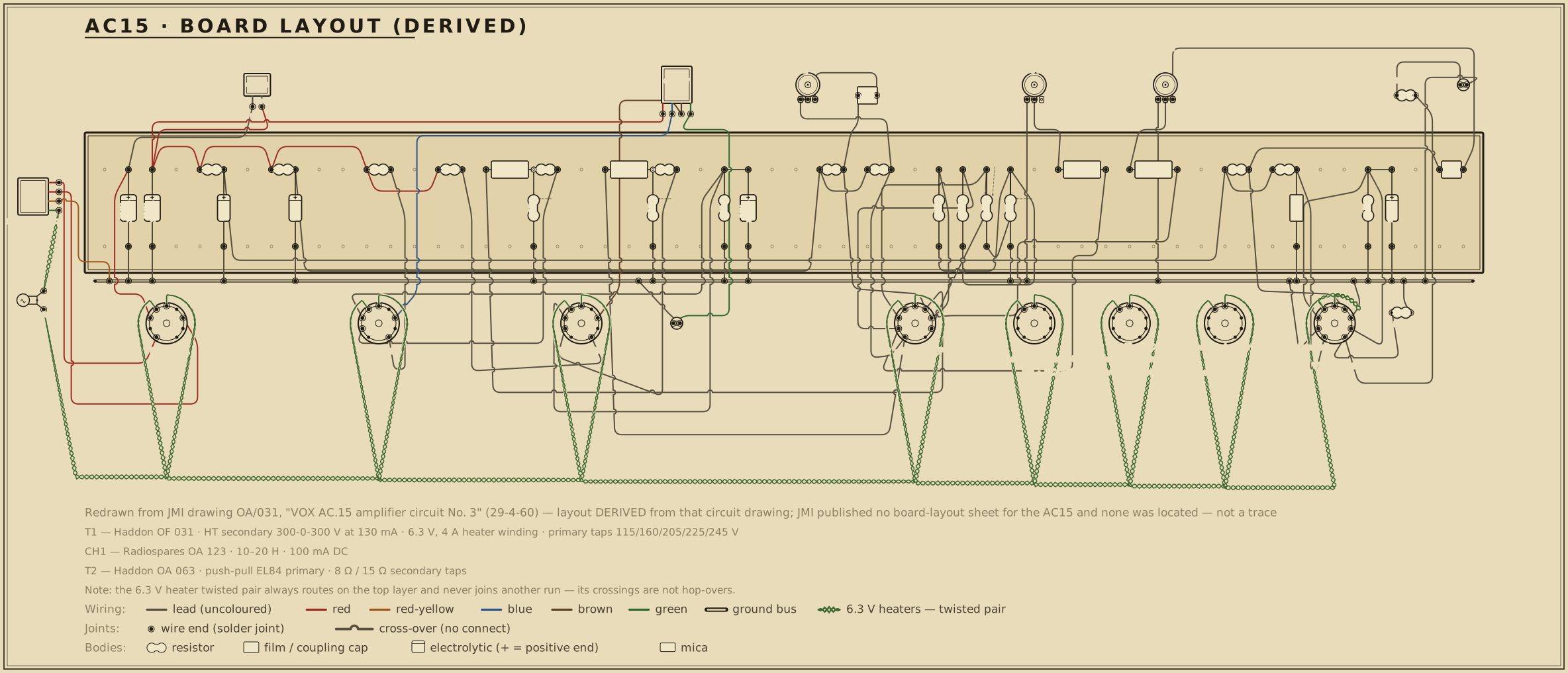
Board layout — redrawn reference diagram · source noted on the drawing Print sheet ↗
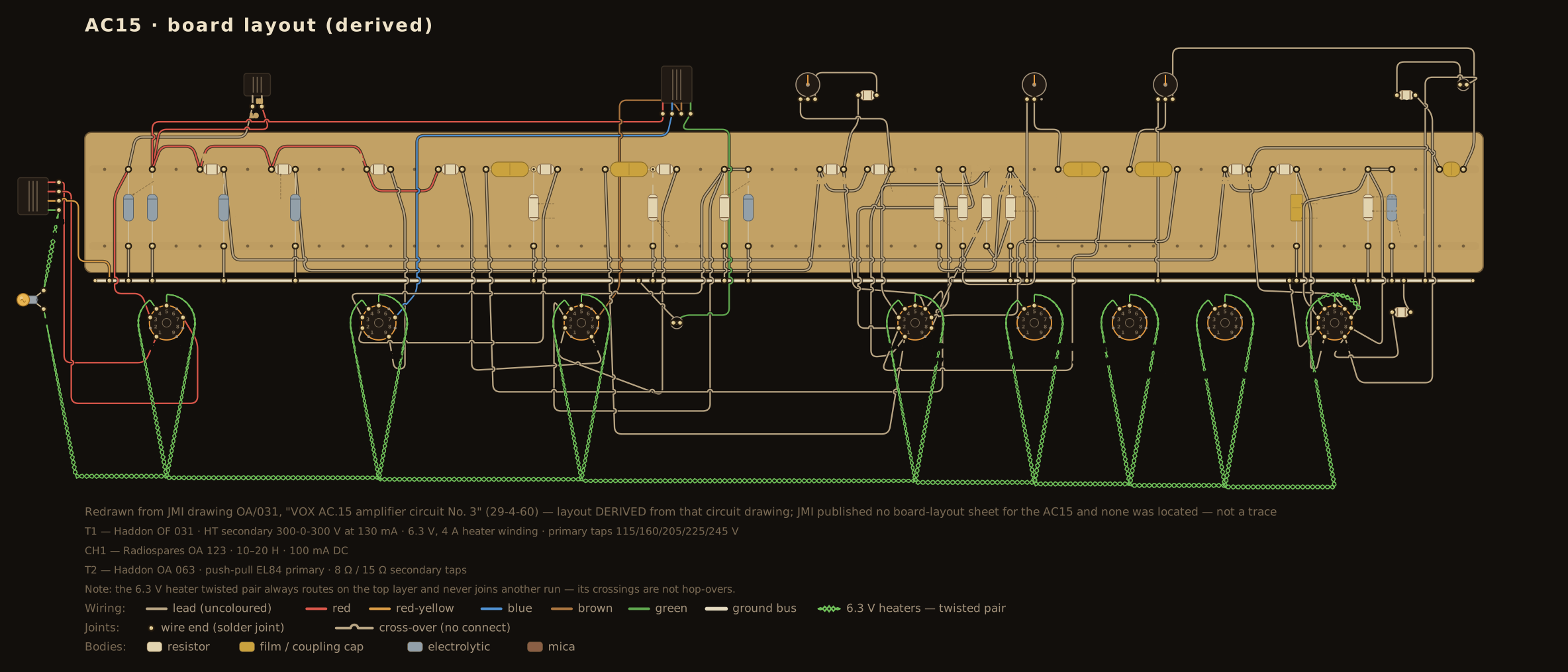
AC15 board layout — an original diagram reconstructed from the redrawn schematic (no factory layout sheet exists), showing the principal parts in board order, drawn in the period layout-sheet style with each value lettered on the part.

Scroll the drawing sideways to read the whole board — the source line and the colour legend run along the bottom of the sheet — or open the full-size diagram in its own tab. Values are lettered on the parts in the period shorthand — .02-400, 250-5, 1MEG: how to read it.

Machine-checked wiring. Every modelled part the operating-point netlist places on this board has been verified in CI, terminal for terminal, to be electrically equivalent to the circuit's simulated netlist. This diagram documents connectivity and part arrangement — it is not a dimensioned 1:1 build template.

Details

The modelled parts are the tube sockets, the plate, cathode and grid-leak resistors, the power-rail droppers, and the coupling and bypass capacitors whose two leads are both named DC nodes; the check proves the same net structure, with no missing or extra connections. Parts outside that DC model — the volume / tone / mixer control-network internals, the negative-bias front end, and the heater chain, pilot lamp and power-transformer / rectifier AC side — are drawn from the cited sources but are not machine-checked; the CI report enumerates every one of their terminals so the boundary is explicit rather than silent.

Board and part positions are drawn at diagram scale, and lead dress, grounding paths, and physical spacing all matter in a high-voltage chassis. If you build from it, verify every connection against the schematic above and the operating-point table below as you go.

Operating point vs. published chart

Chart values read from the published drawing — or, where the drawing carries no voltage chart, from the cited published measurements (never reproduced). The simulated column is this circuit's own netlist solved in ngspice by the run that gates it; every deviation beside it is those two numbers compared, not a separately stated figure. Tolerances are this project's verification targets: tube-pin nodes carry the tolerance the cited source states, or ±20% — the era's printed convention — where it states none, and power rails are held to tighter internal targets.

Node Chart Simulated Deviation Tolerance Note
BPN 289.1 V Normal-channel supply node, after the 22 kΩ dropper from the +315 V rail (8 µF smoothed)
BPPI 287.0 V phase-inverter supply node, after its own 22 kΩ dropper from the +315 V rail (8 µF smoothed)
PEF 90 V 66.3 V 26.3% ±20% EF86 anode — 220 kΩ load. Simulation runs about a quarter low against the printed +90 V; the verification note below explains why the gap sits in the tube model rather than the circuit
SEF 124.8 V EF86 screen grid, fed through 1 MΩ and bypassed by 0.1 µF — the pentode's gain-setting node
KEF 2.6 V EF86 cathode (2.2 kΩ, 25 µF bypass)
PPIA 220 V 223.4 V 1.5% ±20% phase-inverter anode, Normal-channel side (100 kΩ load)
PPIB 220 V 223.4 V 1.5% ±20% phase-inverter anode, Vibrato/Tremolo side (100 kΩ load) — the drawing prints one figure for the pair
KPI 61.3 V phase-inverter shared cathode, above the 1.2 kΩ resistor
JPI 59.8 V tail junction over the 47 kΩ tail — the return for both 1 MΩ grid leaks
S3 314.6 V EL84 screen grid, through its 100 Ω stopper from the rail
S4 314.6 V EL84 screen grid, through its 100 Ω stopper from the rail
KOUT 11.2 V shared EL84 cathode over the single 130 Ω resistor (50 µF bypass) — the amp's entire bias arrangement

Tube-pin nodes are checked at the tolerance the cited source states, or at the era's ±20% convention where it states none; power-rail nodes are held to tighter internal verification targets. Simulated figures are the netlist's DC solution, not measurements from a chassis.

The output stage behind these numbers can be drawn: the load line explorer plots this circuit's EL84 pair at the DC operating point its netlist carries — 315 V on the plates with a 130 Ω cathode resistor — and marks where the load line crosses. This circuit is published as a draft, so that operating point is not verified against a published chart: the table and notes above say what each figure rests on.

Parts list

Every designator in this list appears on the schematic above, and every designator on the schematic appears here — the two are checked against each other in both directions, a valve's two halves counting as one bottle (V1A and V1B are both V1). Twelve parts the drawing carries as annotations rather than numbered symbols are listed here without designators, and stand outside that check. Where the factory drawing and the published redraw give different values for the same part, the FACTORY value is listed and the redraw's modern equivalent noted alongside. Coupling and cathode-bypass capacitor VALUES are open at DC and do not enter the operating-point netlist; they are listed for completeness. Parts belonging to the Vibrato/Tremolo channel are marked — that channel is outside the DC netlist's scope (see notes.md), so its values are read from the drawing but not simulated; the parts of it whose wiring the published scan does not resolve carry no designator and are drawn on the schematic as annotation, not as asserted connections. Asterisked values on the drawing mark the alternate parts for the AC15 Bass; the Normal-voicing values are the ones listed.

RefPartValue / ratingRole
JN1 Jack socket 1/4 in Normal channel input (dual-jack arrangement)
JN2 Jack socket 1/4 in Normal channel input (dual-jack arrangement)
RIN1 Carbon comp resistor 68 kΩ · ½ W Normal channel input grid stopper, dual-jack arrangement
RIN2 Carbon comp resistor 68 kΩ · ½ W Normal channel input grid stopper, dual-jack arrangement
JN Jack socket 1/4 in Normal channel input (single-jack arrangement, drawn as the alternate)
RGS1 Carbon comp resistor 33 kΩ · ½ W Normal channel grid stopper, single-jack arrangement
RG1 Carbon comp resistor 1 MΩ · ½ W Normal channel input grid leak
JV1 Jack socket 1/4 in Vibrato/Tremolo channel input (dual-jack arrangement)
JV2 Jack socket 1/4 in Vibrato/Tremolo channel input (dual-jack arrangement)
RIN3 Carbon comp resistor 68 kΩ · ½ W Vibrato/Tremolo input grid stopper
RIN4 Carbon comp resistor 68 kΩ · ½ W Vibrato/Tremolo input grid stopper
JV Jack socket 1/4 in Vibrato/Tremolo channel input (single-jack arrangement)
RGS2 Carbon comp resistor 33 kΩ · ½ W Vibrato/Tremolo grid stopper, single-jack arrangement
RG2 Carbon comp resistor 1 MΩ · ½ W Vibrato/Tremolo input grid leak
RD1 Power resistor 22 kΩ · 3 W Rail dropper, +315 V → Normal-channel supply node
CF1 Electrolytic capacitor 8 µF Normal-channel supply smoothing
RL1 Carbon comp resistor 220 kΩ · ½ W EF86 anode load
RS1 Carbon comp resistor 1 MΩ · ½ W EF86 screen-grid feed
CS1 Film capacitor 0.1 µF EF86 screen-grid bypass
RK1 Carbon comp resistor 2.2 kΩ · ½ W EF86 cathode bias
CK1 Electrolytic capacitor 25 µF EF86 cathode bypass
CO1 Coupling capacitor 0.01 µF EF86 anode → Brilliance switch → Normal volume
SWBRIL Toggle switch SPST Brilliance switch — closed it shorts CBR out for full-range coupling, open it leaves CBR in circuit (panel-marked for the Normal channel)
CBR Mica capacitor 250 pF Series treble-only coupling cap, bridged by the Brilliance switch (the published redraw prints 220 pF)
VR1 Log potentiometer 500 kΩ Normal channel volume
RD2 Power resistor 22 kΩ · 3 W Rail dropper, +315 V → phase-inverter supply node
CF2 Electrolytic capacitor 8 µF Phase-inverter supply smoothing
CIN1 Coupling capacitor 0.01 µF Normal volume → phase-inverter grid (side A)
CIN2 Coupling capacitor 0.01 µF Vibrato/Tremolo volume → phase-inverter grid (side B)
RLA Carbon comp resistor 100 kΩ · ½ W Phase-inverter anode load (side A)
RLB Carbon comp resistor 100 kΩ · ½ W Phase-inverter anode load (side B)
RGA Carbon comp resistor 1 MΩ · ½ W Phase-inverter grid leak (side A), returned to the tail junction
RGB Carbon comp resistor 1 MΩ · ½ W Phase-inverter grid leak (side B), returned to the tail junction
RTAIL Carbon comp resistor 1.2 kΩ · ½ W Phase-inverter shared cathode resistor
RT2 Carbon comp resistor 47 kΩ · ½ W Phase-inverter tail (junction → ground)
VR3 Log potentiometer 250 kΩ Top Cut — in series with a cap across the two phase-inverter outputs
CTC Film capacitor 0.005 µF Top Cut capacitor (the published redraw prints 0.0047 µF)
CC1 Coupling capacitor 0.01 µF Phase inverter → EL84 grid (upper)
CC2 Coupling capacitor 0.01 µF Phase inverter → EL84 grid (lower)
RGL1 Carbon comp resistor 220 kΩ · ½ W EL84 grid leak (upper), returned to ground
RGL2 Carbon comp resistor 220 kΩ · ½ W EL84 grid leak (lower), returned to ground
RST1 Carbon comp resistor 1.5 kΩ · ½ W EL84 grid stopper (upper)
RST2 Carbon comp resistor 1.5 kΩ · ½ W EL84 grid stopper (lower)
RSC1 Power resistor 100 Ω · 3 W EL84 screen-grid stopper (upper)
RSC2 Power resistor 100 Ω · 3 W EL84 screen-grid stopper (lower)
R22 Power resistor 130 Ω · 5 W SHARED EL84 cathode bias resistor — the whole bias arrangement for the pair (factory designator; the published redraw prints a 10 W part)
CKO Electrolytic capacitor 50 µF · 50 V EL84 cathode bypass (the published redraw prints 47 µF)
RD3 Power resistor 22 kΩ · 3 W Vibrato/Tremolo channel rail dropper from +315 V
CF3 Electrolytic capacitor 33 µF Vibrato/Tremolo supply smoothing
RKV1 Carbon comp resistor 2.2 kΩ · ½ W Vibrato/Tremolo first-stage cathode bias
CKV1 Electrolytic capacitor 25 µF Vibrato/Tremolo first-stage cathode bypass
RKV2 Carbon comp resistor 1.5 kΩ · ½ W Vibrato/Tremolo second-stage cathode bias
RGV Carbon comp resistor 1 MΩ · ½ W Vibrato/Tremolo inter-stage grid return
CVC Coupling capacitor 0.01 µF Vibrato/Tremolo inter-stage coupler
VR2 Log potentiometer 500 kΩ Vibrato/Tremolo channel volume
Carbon comp resistor 150 kΩ · ½ W Vibrato/Tremolo supply dropper (annotation only)
Carbon comp resistor 12 kΩ · ½ W Vibrato/Tremolo supply dropper (annotation only)
Carbon comp resistor 22 kΩ · ½ W Vibrato/Tremolo supply dropper (annotation only)
Tone network (2 positions) 0.0022 µF / 500 pF · 68 kΩ · 330 kΩ · 500 pF / 100 pF · 22 kΩ TONE I / TONE II — the switched two-position voicing network of the Vibrato/Tremolo channel (annotation only)
Phase-shift ladder 5 × 0.0047 µF with 4 × 1 MΩ The vibrato phase-shift chain feeding the Vibrato/Tremolo volume (annotation only)
Modulator network 470 kΩ · 1 MΩ · 180 kΩ · 10 kΩ · 1.5 kΩ · 47 kΩ · 0.1 µF · 220 pF · 0.033 µF ECC82 modulator around the phase-shift ladder (annotation only)
Oscillator network 3 × 0.01 µF with 1 MΩ returns · 220 kΩ · 270 kΩ · 560 kΩ · 22 kΩ · 1.5 kΩ · 3.9 kΩ · 25 µF · 0.1 µF · 0.022 µF ECC83 phase-shift oscillator — the vibrato/tremolo generator (annotation only)
Potentiometer 1 MΩ Depth (annotation only)
Potentiometer 3 MΩ Speed (annotation only)
Toggle switch SPST Vibrato/Tremolo speed fast/slow — on the back of the Depth pot (annotation only)
Footswitch SPST Vibrato/Tremolo on/off, remote (annotation only)
Jack socket 1/4 in Footswitch jack (annotation only)
V1 Preamp tube EF86 Normal channel pentode preamp
V2 Preamp tube ECC83 (12AX7) Long-tailed-pair phase inverter — both channels mix here
V3 Power tube EL84 Push-pull output (upper)
V4 Power tube EL84 Push-pull output (lower)
V5 Preamp tube ECC83 (12AX7) Vibrato/Tremolo channel first stage
V6 Preamp tube ECC82 (12AU7) Vibrato/Tremolo modulator
V7 Preamp tube ECC83 (12AX7) Vibrato/Tremolo phase-shift oscillator
V8 Rectifier tube EZ81 (6CA4) Full-wave rectifier
T1 Power transformer Haddon OF 031 · HT secondary 300-0-300 V at 130 mA · 6.3 V, 4 A heater winding · primary taps 115/160/205/225/245 V Mains/HT transformer
T2 Output transformer Haddon OA 063 · push-pull EL84 primary · 8 Ω / 15 Ω secondary taps Output transformer
CH1 Filter choke Radiospares OA 123 · 10–20 H · 100 mA DC Smoothing choke between reservoir and HT rail
CR1 Electrolytic capacitor 16 µF · 450 V Reservoir filter, EZ81 cathode side
CR2 Electrolytic capacitor 16 µF · 450 V Smoothing filter after the choke
SW1 Toggle switch DPST Mains on/off
SW2 Rotary switch 5-position Mains voltage selector — 115/160/205/225/245 V
SW7 Toggle switch SPST Standby — breaks the HT rail after the smoothing choke
F1 Fuse 2 A Mains fuse — value from the published redraw; the factory scan does not resolve this figure
PL1 Pilot lamp 6.3 V Panel pilot lamp
JSPK1 Jack socket 1/4 in Speaker output
JSPK2 Jack socket 1/4 in Speaker output (second)

Circuit story

The AC15 was Jennings Musical Industries' first guitar amplifier, a British 15-watt combo from the end of the 1950s, and the circuit documented here is its third revision: JMI drawing OA/031, "VOX AC.15" amplifier circuit No. 3, drawn on 29 April 1960 and signed off by Dick Denney. It is the version that put the phase-shifting vibrato back inside the amplifier rather than in a box on the back, and it stayed in production, unchanged as a circuit, into 1963.

Almost nothing about it is done the way an American amplifier of the same year does it. There is no tone stack. There is no bias supply. The two channels do not mix before the phase inverter — they mix inside it. The first valve is a pentode, not a triode. Every one of those choices is audible.

Circuit walkthrough (short form)

Normal channel. Input (33 kΩ stopper, 1 MΩ leak) → EF86 pentode, running a 220 kΩ anode load, a 1 MΩ screen feed bypassed by 0.1 µF, and a 2.2 kΩ cathode resistor with a 25 µF bypass. This is not a Vox invention: it is Philips' own published application circuit for the valve, reproduced part for part — the datasheet tabulates a voltage gain near 200 for exactly this network, several times what a triode stage delivers in the same place. The anode couples out through 0.01 µF into the Brilliance switch, and from there to a 500 kΩ volume control. The switch works on a 250 pF capacitor sitting in series with that signal path: leave the switch open and everything has to cross the small cap, so only the top end gets through; close it and the cap is shorted out, restoring the full-range coupling.

Vibrato/Tremolo channel. Its own input valve (ECC83) and a two-position tone network feed a phase-shift ladder of five 0.0047 µF capacitors and four 1 MΩ returns. An ECC82 modulator swings that ladder under the control of an ECC83 phase-shift oscillator with Speed and Depth controls and a footswitch — the circuit Vox called Vibravox. Because the ladder shifts phase rather than simply gating level, this is closer to true vibrato than the amplitude tremolo of its American contemporaries.

Phase inverter. Both channels arrive here, at a long-tailed pair (ECC83, 100 kΩ anode loads, a 1.2 kΩ shared cathode resistor over a 47 kΩ tail, both 1 MΩ grid leaks returned to the tail junction) — but not at the same grid. The Normal volume drives one side, the Vibrato/Tremolo volume drives the other, so the two channels are summed by the inverter itself. Playing into both inputs at once is therefore not quite the parallel blend it would be in a Fender: the channels enter in opposite phase.

Top Cut. The amp's only tone control, and it sits after the inverter, not before it: a 250 kΩ pot in series with a 0.005 µF cap, bridged across the two inverter outputs. Turning it up shunts treble differentially between the two phases, so it darkens both channels at once, downstream of everything.

Output. Two EL84 pentodes, 1.5 kΩ grid stoppers, 220 kΩ grid leaks, and 100 Ω screen stoppers off the same rail as the anodes. Bias is a single shared 130 Ω cathode resistor with a 50 µF bypass — one resistor for the pair, no bias supply and no adjustment — feeding an output transformer with 8 Ω and 15 Ω taps. There is no negative-feedback loop anywhere around the output stage.

Power. An EZ81 rectifier off a 300-0-300 V secondary feeds a 16 µF reservoir, a 10–20 H choke and a second 16 µF can; the standby switch breaks the rail after the choke. Three 22 kΩ / 3 W droppers hang off that +315 V rail, one for each channel and one for the phase inverter. Mains taps run 115 through 245 V; transformers came from Haddon, the choke from Radiospares.

Why it sounds the way it does

Three things carry most of the character. The EF86 front end supplies gain a triode cannot, so the amp is already working hard at modest volume. The output pair is cathode-biased and carries no feedback loop, which lets the stage compress and bloom instead of stiffening up. And the Top Cut sits at the inverter rather than in the preamp, so the top end is trimmed after the amp has done its distorting — the reason a rolled-off AC15 still sounds bright-edged rather than muffled.

The EF86 is also the amp's fragile part. It is a high-gain small-signal pentode in a combo cabinet with a 12-inch speaker, and it is famously microphonic in that job. It survived the scale-up: the first AC30/6, drawn on the same day as this amp's own sheet, kept the EF86 on its Normal channel. It was the revision of May 1961 that dropped it, replacing it with an ECC83 for exactly that reason — in a louder cabinet the valve's sensitivity to vibration had become the amplifier's weak point.

A note on verification

The factory drawing annotates five working voltages — +325 V at the reservoir, +315 V at the rail, +90 V at the EF86 anode, +220 V at the phase-inverter anode and +310 V at the EL84 anodes — but prints no tabulated valve-voltage chart, so there is no per-pin reference and no stated measurement convention behind them. Simulated from the redrawn netlist, the phase inverter lands within 2% of its printed figure and the output stage settles at an entirely believable 11 V of cathode bias. The EF86 anode does not: it simulates about a quarter low. That gap is in the tube model, not the circuit — Philips' own tabulated figures for this exact resistor network predict an anode within a few volts of the printed +90 V, while the archive's single-anchor EF86 model draws roughly 10% more cathode current at this far-from-datasheet operating point, and a 220 kΩ anode load turns 10% of current into a quarter of the voltage.

The circuit is therefore published as a draft. Its topology and part values are read from the factory drawing and cross-checked against two independent published readings of the same circuit; its operating point is not yet confirmed end to end.

The DC netlist covers the Normal channel, the phase inverter and the output stage. The Vibrato/Tremolo channel is documented in the parts list but left out of the simulation: its oscillator has no static operating point to solve for, and reporting a partial answer for that side of the amp would be worse than reporting none.

A note on the drawings

The redrawn schematic asserts every connection the published drawing resolves: the Normal channel, the phase inverter, the Top Cut, the output stage and the power supply. The Vibrato/Tremolo channel's tone, phase-shift, modulator and oscillator networks are inventoried part by part in the parts list, but the available scan does not resolve how those parts interconnect, so the schematic names the interfaces each valve works into and asserts nothing further.

The board layout is derived. JMI published no board-layout sheet for the AC15, and none has been located, so the diagram lays this circuit's own parts out in signal order along the chassis on the house eyelet grid — a builder's reference for the circuit rather than a record of the factory's tag-strip construction, which is what the amplifier actually used. Its point-to-point wiring is nonetheless machine-checked: every part the operating-point netlist models is verified in CI, terminal for terminal, to sit on the same nets the simulation solves.

Sources