AA1164 Blackface Princeton Reverb‑style · 1964–1967 · 12 W

✓ verified 2026-08-02
Schematic — redrawn in KiCad · scroll to zoom, drag to pan
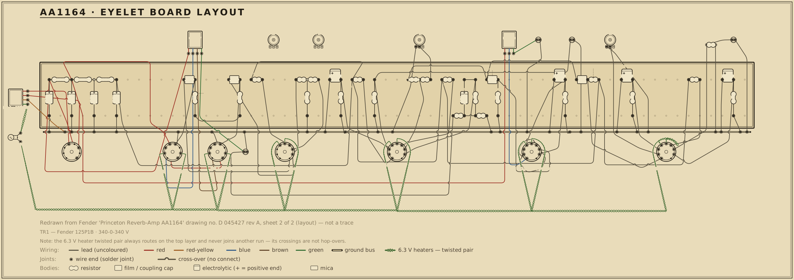
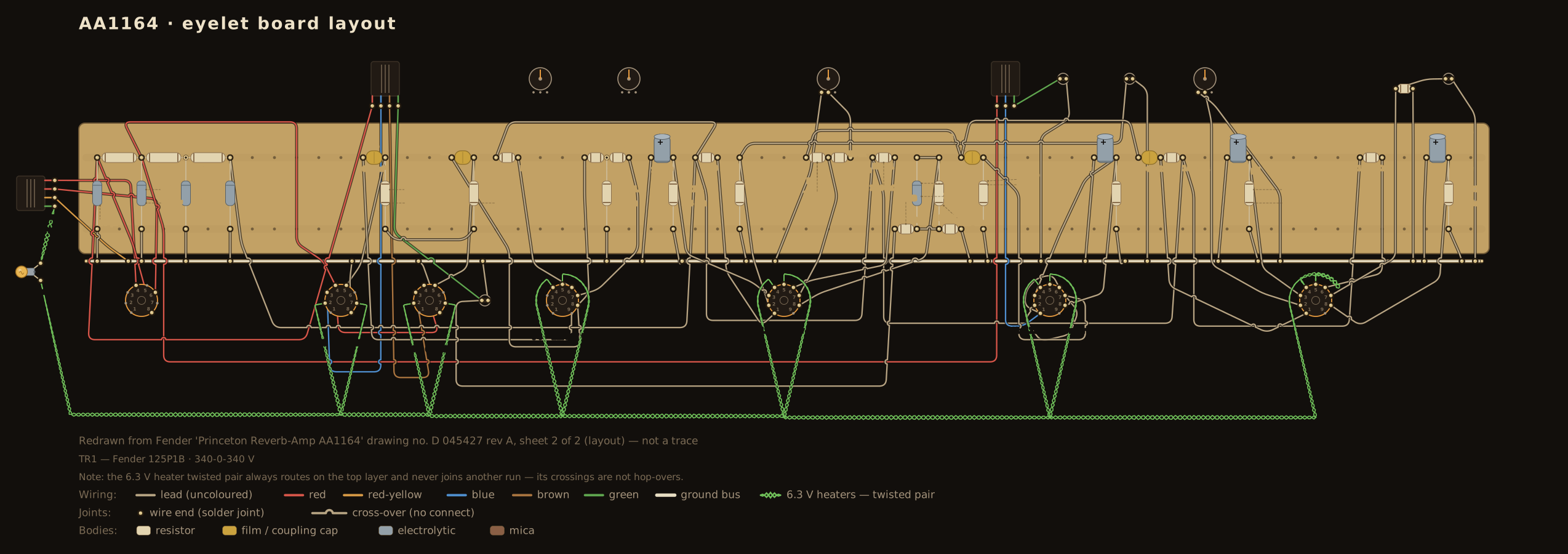
Board layout — redrawn reference diagram · source noted on the drawing Print sheet ↗
AA1164 eyelet board layout — an original diagram redrawn from the published layout drawing, showing the principal parts in the order that drawing places them on the board, drawn in the period layout-sheet style with each value lettered on the part.

Scroll the drawing sideways to read the whole board — the source line and the colour legend run along the bottom of the sheet — or open the full-size diagram in its own tab. Values are lettered on the parts in the period shorthand — .02-400, 250-5, 1MEG: how to read it.

Machine-checked wiring. Every modelled part the operating-point netlist places on this board has been verified in CI, terminal for terminal, to be electrically equivalent to the simulated netlist this circuit is verified against. This diagram documents connectivity and part arrangement — it is not a dimensioned 1:1 build template.

Details

The modelled parts are the tube sockets, the plate, cathode and grid-leak resistors, the power-rail droppers, and the coupling and bypass capacitors whose two leads are both named DC nodes; the check proves the same net structure, with no missing or extra connections. Parts outside that DC model — the volume / tone / mixer control-network internals, the negative-bias front end, and the heater chain, pilot lamp and power-transformer / rectifier AC side — are drawn from the cited sources but are not machine-checked; the CI report enumerates every one of their terminals so the boundary is explicit rather than silent.

Board and part positions are drawn at diagram scale, and lead dress, grounding paths, and physical spacing all matter in a high-voltage chassis. If you build from it, verify every connection against the schematic above and the operating-point table below as you go.

Operating point vs. published chart

Chart values read from the published drawing — or, where the drawing carries no voltage chart, from the cited published measurements (never reproduced). The simulated column is this circuit's own netlist solved in ngspice by the run that gates it; every deviation beside it is those two numbers compared, not a separately stated figure. Tolerances are this project's verification targets: tube-pin nodes carry the tolerance the cited source states, or ±20% — the era's printed convention — where it states none, and power rails are held to tighter internal targets. Every gated node lands within target — worst deviation 11.5%.

Node Chart Simulated Deviation Tolerance Note
BB 400 V 407.5 V 1.9% ±8% screen / reverb-driver rail, solved through the 1 kΩ-1 W dropper from the +420 reservoir
BC 320 V 327.6 V 2.4% ±8% middle supply node between the two 18 kΩ-1 W droppers; nothing else taps it, so the chart's two 80 V drops must match
BD 240 V 247.7 V 3.2% ±8% preamp and phase-inverter rail, after the second 18 kΩ-1 W dropper
PN1 160 V 160.8 V 0.5% ±20% preamp input-stage plate, 100 kΩ from +240
KN1 1.3 V 1.3 V 0.2% ±20% preamp input-stage cathode over 1.5 kΩ
PN2 160 V 160.8 V 0.5% ±20% preamp second-stage plate, 100 kΩ from +240
KN2 1.3 V 1.3 V 0.2% ±20% preamp second-stage cathode over 1.5 kΩ
PRD 400 V 406.8 V 1.7% ±20% reverb-driver 12AT7 plate (paralleled sections), off the screen rail through the TR3 primary DCR
KRD 8 V 8.0 V 0.0% ±20% reverb-driver 12AT7 shared cathode over 2.2 kΩ
PR1 160 V 160.8 V 0.5% ±20% reverb-recovery plate, 100 kΩ from +240
KR1 1.2 V 1.3 V 8.6% ±20% reverb-recovery cathode over 1.5 kΩ
PD1 160 V 162.0 V 1.3% ±20% driver / mixer plate, 100 kΩ from +240
KD1 1.2 V 1.3 V 10.4% ±20% driver / mixer cathode, 1.5 kΩ above the 47 Ω feedback resistor
PPI 200 V 193.0 V 3.5% ±20% split-load phase-inverter plate, 56 kΩ from +240
KPI 50 V 55.6 V 11.2% ±20% split-load phase-inverter cathode, above the 1 kΩ
JPI 49 V 54.6 V 11.5% ±20% phase-inverter 1 kΩ / 56 kΩ junction — the grid-leak return that biases the stage
G61 −34 V −34.0 V 0.0% ±8% 6V6 (V5) grid, fixed bias through the 220 kΩ-5% leak from the −34 V supply

Tube-pin nodes are checked at the tolerance the cited source states, or at the era's ±20% convention where it states none; power-rail nodes are held to tighter internal verification targets. Simulated figures are the netlist's DC solution, not measurements from a chassis.

The output stage behind these numbers can be drawn: the load line explorer plots this circuit's 6V6GT pair at the DC operating point its netlist carries — 420 V on the plates with a −34 V grid bias — and marks where the load line crosses.

Parts list

Every designator in this list appears on the schematic above, and every designator on the schematic appears here — the two are checked against each other in both directions, a valve's two halves counting as one bottle (V1A and V1B are both V1). The drawing shows one jack symbol for the instrument input pair; the chassis carries two. Tube reference designators run from the input end of the chassis (V1 nearest the jacks) — the drawing labels socket types, not V-numbers, and the section split shown here is read off the layout sheet's per-pin voltages. Tremolo-oscillator and reverb-tank interconnect parts are listed, but the oscillator's DC point is excluded from the netlist (see notes.md). The 125P1B is the power transformer Fender shared across the Champ, the Princeton and the Princeton Reverb, and the HT winding is not annotated the same way on every sheet: this drawing prints 340-0-340 V, as does the Princeton AA964, while the Champ AA764 sheet prints 320-0-320 V for the same part number. Each entry records the figure its own drawing prints.

RefPartValue / ratingRole
R1a Carbon comp resistor 68 kΩ · ½ W Input grid stopper (jack 1)
R1b Carbon comp resistor 68 kΩ · ½ W Input grid stopper (jack 2)
RGN1 Carbon comp resistor 1 MΩ · ½ W Input grid leak
RLN1 Carbon comp resistor 100 kΩ · ½ W V1a plate load
RKN1 Carbon comp resistor 1.5 kΩ · ½ W V1a cathode bias
CKN1 Electrolytic capacitor 25 µF · 25 V V1a cathode bypass
CT Mica capacitor 250 pF Treble cap
VRT Audio-taper potentiometer 250 kΩ-A Treble
RS Carbon comp resistor 100 kΩ · ½ W Tone-stack slope resistor
CB1 Coupling capacitor 0.1 µF Tone-stack bass cap, slope node to the bass pot
VRB Audio-taper potentiometer 250 kΩ-A Bass
CB2 Coupling capacitor 0.047 µF Tone-stack middle-leg cap, slope node to the bleed resistor
RSL Carbon comp resistor 6.8 kΩ · ½ W Tone-stack bleed resistor
VRVOL Audio-taper potentiometer 1 MΩ-A Volume
RLN2 Carbon comp resistor 100 kΩ · ½ W V1b plate load
RKN2 Carbon comp resistor 1.5 kΩ · ½ W V1b cathode bias
CKN2 Electrolytic capacitor 25 µF · 25 V V1b cathode bypass
CC1 Coupling capacitor 0.02 µF V1b output coupling
RMIX Carbon comp resistor 3.3 MΩ · ½ W Dry-signal mixing resistor into the driver grid
CMIX Mica capacitor 10 pF Bright cap across the dry mixing resistor
RMR Carbon comp resistor 470 kΩ · ½ W Reverb mixing resistor (Reverb wiper → driver grid)
CRS Coupling capacitor 500 pF Reverb send coupling to the driver grid
RGRD Carbon comp resistor 1 MΩ · ½ W Reverb-driver grid leak
RKRD Carbon comp resistor 2.2 kΩ · ½ W Reverb-driver shared cathode bias
CKRD Electrolytic capacitor 25 µF · 25 V Reverb-driver cathode bypass
TR3 Reverb transformer Fender 125A20B Reverb driver → tank input
TANK Reverb tank spring reverb unit Reverb delay line (input and output jacks)
RGR1 Carbon comp resistor 220 kΩ · ½ W Reverb-recovery grid resistor (tank output)
RLR1 Carbon comp resistor 100 kΩ · ½ W V3a plate load
RKR1 Carbon comp resistor 1.5 kΩ · ½ W V3a cathode bias
CKR1 Electrolytic capacitor 25 µF · 25 V V3a cathode bypass
CCR1 Coupling capacitor 0.003 µF Reverb-recovery output coupling
VRREV Linear potentiometer 100 kΩ-L Reverb
RLD1 Carbon comp resistor 100 kΩ · ½ W V3b plate load
RKD1 Carbon comp resistor 1.5 kΩ · ½ W V3b cathode bias (bypassed)
CKD1 Electrolytic capacitor 25 µF · 25 V V3b cathode bypass
RKD2 Carbon comp resistor 47 Ω · ½ W V3b unbypassed cathode resistor / feedback injection point
RNFB Carbon comp resistor 2.7 kΩ · ½ W Negative feedback, speaker → driver cathode
CC2 Coupling capacitor 0.02 µF Driver → phase-inverter coupling
RLPI Carbon comp resistor 56 kΩ · ½ W Phase-inverter plate load
RKPI Carbon comp resistor 1 kΩ · ½ W Phase-inverter cathode bias resistor
RTAIL Carbon comp resistor 56 kΩ · ½ W Phase-inverter cathode load
RGPI Carbon comp resistor 1 MΩ · ½ W Phase-inverter grid leak, returned to the 1 kΩ / 56 kΩ junction
C1 Coupling capacitor 0.1 µF · 400 V Inverter plate → V5 grid
C2 Coupling capacitor 0.1 µF · 400 V Inverter cathode → V6 grid
RTOP Carbon comp resistor 220 kΩ · ½ W Tremolo oscillator plate load
RKTO Carbon comp resistor 3.3 kΩ · ½ W Tremolo oscillator cathode bias
CKTO Electrolytic capacitor 25 µF · 25 V Tremolo oscillator cathode bypass
CTO1 Film capacitor 0.02 µF Tremolo oscillator plate coupling
CTO2 Film capacitor 0.05 µF Tremolo phase-shift cap
CTO3 Film capacitor 0.01 µF Tremolo phase-shift cap (Speed network)
RTO1 Carbon comp resistor 1 MΩ · ½ W Tremolo phase-shift resistor to ground
RTO2 Carbon comp resistor 1 MΩ · ½ W Tremolo phase-shift resistor to the oscillator cathode
RSPD Carbon comp resistor 100 kΩ · ½ W Speed-network series resistor
VRSPD Reverse-audio potentiometer 3 MΩ-RA Speed
RTOUT Carbon comp resistor 1 MΩ · ½ W Tremolo oscillator output series resistor
CTO4 Film capacitor 0.02 µF Tremolo output shunt to ground
CINT Coupling capacitor 0.1 µF Tremolo output coupling into the Intensity control
VRINT Linear potentiometer 250 kΩ-L Intensity — sets how far the oscillator swings the bias line
RGL1 Carbon comp resistor 220 kΩ · ½ W · 5% V5 grid leak, from the −34 V bias line
RGL2 Carbon comp resistor 220 kΩ · ½ W · 5% V6 grid leak, from the −34 V bias line
TR2 Output transformer Fender 125A10B Push-pull 6V6 output
JEXT Jack external speaker Parallel speaker output
RB1 Carbon comp resistor 100 kΩ · ½ W · 5% Bias-supply feed from the HT winding
DB1 Rectifier (bias) silicon diode Bias-supply rectifier
CB3 Electrolytic capacitor 25 µF · 50 V Bias-supply filter
RB2 Carbon comp resistor 22 kΩ · ½ W Bias-supply bleeder
TR1 Power transformer Fender 125P1B · 340-0-340 V HT + heaters + rectifier filament
CF1 Electrolytic capacitor 20 µF · 450 V Reservoir filter (+420 V, OT centre tap)
R1K Wirewound resistor 1 kΩ · 1 W Dropper, reservoir → screen rail
CF2 Electrolytic capacitor 20 µF · 450 V Filter, screen rail (+400 V)
RD1 Wirewound resistor 18 kΩ · 1 W Dropper, screen rail → +320 V node
CF3 Electrolytic capacitor 20 µF · 450 V Filter, +320 V node
RD2 Wirewound resistor 18 kΩ · 1 W Dropper, +320 V → preamp rail
CF4 Electrolytic capacitor 20 µF · 450 V Filter, preamp / phase-inverter rail (+240 V)
RH1 Carbon comp resistor 100 Ω · ½ W Heater hum-balance resistor
RH2 Carbon comp resistor 100 Ω · ½ W Heater hum-balance resistor
F1 Fuse 1 A slo-blo Mains fuse
SW1 Switch SPST AC switch
SW2 Switch SPDT Ground switch (period; not in modern builds)
CDEATH Ceramic capacitor 0.047 µF · 600 V Ground-switch cap (period; not in modern builds)
JVIB Jack vibrato footswitch Grounds the oscillator to switch the tremolo off
JREV Jack reverb footswitch Reverb footswitch
V1 Preamp tube 12AX7 (7025) Preamp input stage + second stage (V1a/V1b)
V2 Preamp/driver tube 12AT7 Reverb driver (both sections paralleled)
V3 Preamp tube 12AX7 Reverb recovery + driver/mixer stage (V3a/V3b)
V4 Preamp tube 12AX7 Tremolo oscillator (DC point excluded) + split-load phase inverter (V4a/V4b)
V5 Power tube 6V6GT Push-pull output (inverter-plate side)
V6 Power tube 6V6GT Push-pull output (inverter-cathode side)
V7 Rectifier tube 5U4GB Full-wave rectifier

Circuit story

The reverb-equipped blackface Princeton: a 12-watt, single-channel amp with tube reverb and a genuine tremolo, running a fixed-biased pair of 6V6GTs behind a split-load phase inverter. It was introduced in 1964 alongside the reverbless AA964 and carried blackface cosmetics through 1967. Six controls — Volume, Treble, Bass, Reverb, Speed, Intensity — and a 5U4GB rectifier rather than the GZ34 of its larger siblings. The preamp bottle is marked 7025 on the drawing, the low-noise selected version of the 12AX7.

Signal path

Preamp. Two inputs, each through its own 68 kΩ stopper onto a shared 1 MΩ grid leak → first 12AX7 stage (100 kΩ plate load, 1.5 kΩ cathode with a 25 µF bypass) → a treble-bass tone stack (250 kΩ treble and bass, a 100 kΩ slope resistor, 6.8 kΩ bleed, 250 pF, 0.1 µF and 0.047 µF caps) and a 1 MΩ Volume → a second identical 12AX7 stage. There is only one channel; everything the amp does happens in this one chain.

The tone stack, as the sheet wires it. The AA1164 draws the same two-knob ladder as the AA964 it descends from — not the textbook redrawing of the same parts — and the schematic here follows the sheet (re-read at lug level 2026-08-03): the 250 pF and the 100 kΩ slope both leave the plate node; the 0.1 µF runs from the slope foot to the node shared by the treble pot's lower lug and the bass pot; the bass pot is a rheostat above the 0.047 µF/6.8 kΩ foot (the factory layout mounts the 6.8 kΩ right on the bass pot, its far lead grounded to the case); and the stack's output is the treble pot's wiper alone, into the Volume control. The tone-stack lab plots this circuit with that wiring.

Reverb. After the second preamp stage the signal splits. A 500 pF cap taps the dry signal off to a 12AT7 with both triodes in parallel (2.2 kΩ shared cathode) that swings the 125A20B transformer and the spring tank. The return comes back through a 12AX7 recovery stage (220 kΩ grid resistor, 100 kΩ plate, 1.5 kΩ cathode) and the 100 kΩ Reverb control. Dry and wet are then summed by a pair of resistors straight onto the next grid: 3.3 MΩ for the dry path (with a 10 pF cap across it to keep the top end) and 470 kΩ for the reverb.

Driver. The mixed signal drives a third 12AX7 stage with a 100 kΩ plate load and a two-part cathode: 1.5 kΩ bypassed by 25 µF, sitting on an unbypassed 47 Ω. That 47 Ω is where the negative feedback lands — a 2.7 kΩ resistor back from the speaker — so the whole loop closes on a cathode rather than on the inverter.

Tremolo. A 12AX7 phase-shift oscillator (Speed on a 3 MΩ control) does not touch the audio path at all. Its output is coupled through the 250 kΩ Intensity control directly onto the −34 V bias line feeding the output tubes' grid leaks, so the tremolo works by rocking the output stage's bias up and down. That is a different mechanism from the optocoupler tremolo of the larger blackface amps, which shunts a preamp grid to ground instead.

Phase inverter and output. A single 12AX7 triode wired as a split-load (cathodyne) inverter: 56 kΩ in the plate, 1 kΩ plus 56 kΩ in the cathode, and a 1 MΩ grid leak returned to the junction of those two cathode resistors, which is what sets the stage's bias. Plate and cathode feed the two 6V6GT grids through 0.1 µF caps. The output tubes are fixed-biased at −34 V through 220 kΩ 5% leaks; their screens tie straight to the supply with no screen resistors, and the 125A10B output transformer drives the speaker and a parallel external-speaker jack.

Power

340-0-340 V (power transformer 125P1B) → 5U4GB+420 V at the reservoir, which is also the output transformer's centre tap → a 1 kΩ · 1 W dropper → +400 V for the 6V6 screens and the reverb driver → 18 kΩ · 1 W → +320 V → 18 kΩ · 1 W → +240 V for every preamp plate load and the phase inverter. The 6V6 plates read +410 V, ten volts under the centre tap they hang from. A separate negative supply — a 100 kΩ 5% feed off the HT winding, a silicon rectifier, a 25 µF can and a 22 kΩ bleeder — provides the −34 V fixed bias.

Nothing taps the +320 V node except its own filter capacitor, which is why the two 18 kΩ droppers show identical 80 V drops on the printed chart.

What sets it apart

Compared with the reverb-and-tremolo blackface amps above it, the AA1164 makes three different choices.

The phase inverter is a split-load stage rather than a long-tailed pair. A cathodyne has no voltage gain of its own, so all the drive for the output tubes has to come out of the preamp ahead of it, and the two 6V6 grids are fed from one triode instead of two.

The tremolo modulates the output stage's bias instead of shunting a preamp grid through an optocoupler. Its depth therefore depends on where the output tubes are biased rather than on how much signal is at a grid.

The feedback returns to a driver cathode over a 47 Ω resistor rather than to the phase inverter. With only 47 Ω of unbypassed cathode resistance to work against, the loop is a shallow one.

Reading against the printed chart

The drawing prints a full voltage chart, every value set at ±20 %, read to ground with an electronic voltmeter. The simulation takes only the +420 V reservoir as given and solves the 1 kΩ and both 18 kΩ droppers, so the +400 V screen rail, the +320 V node and the +240 V preamp rail are results rather than assumptions — and they land 1.9 %, 2.4 % and 3.2 % from the chart. Below them the preamp plates sit at +161 V against a printed +160 V, the reverb-driver cathode at +8.0 V exactly on the chart, and the split-load inverter's three nodes no more than 12 % from their printed +200 V / +50 V / +49 V.

One node is set aside. The tremolo oscillator shares a bottle with the phase inverter, and its printed pins (+260 V plate, +2.4 V cathode) are the running average a meter reads while it swings, set by grid-leak detection rather than by a static operating point. It is reported rather than fitted to the chart. Its plate load draws about half a milliamp from the screen rail, so leaving it out accounts for roughly half a volt of the margin by which the three supply nodes read high.

Every gated node verifies against the printed chart within the drawing's own ±20 % convention — the worst 11.5 % off — with the tremolo oscillator set aside above as a documented exclusion rather than force-fitted to the chart.

Sources