5G9 Tweed Tremolux‑style · 1957–1960 · 18 W

draft
Schematic — redrawn in KiCad · scroll to zoom, drag to pan
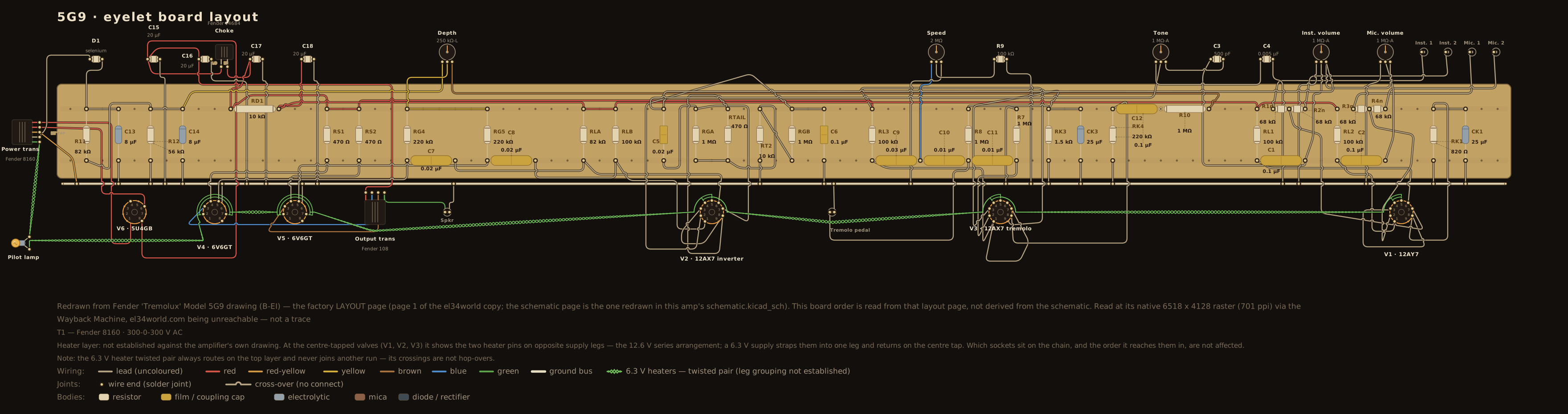
Board layout — redrawn reference diagram · source noted on the drawing Print sheet ↗
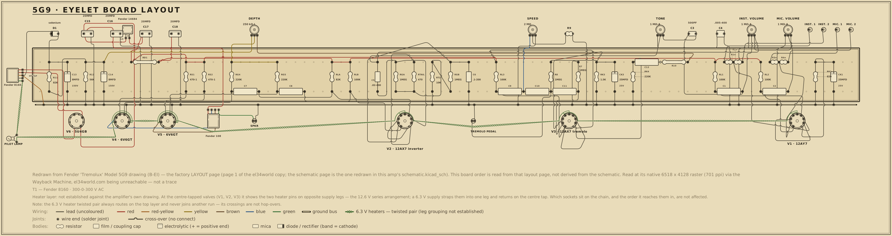
5G9 eyelet board layout — an original diagram reconstructed from this circuit's redrawn schematic rather than from a published layout drawing, showing the principal parts in board order, drawn in the period layout-sheet style with each value lettered on the part.

Scroll the drawing sideways to read the whole board — the source line and the colour legend run along the bottom of the sheet — or open the full-size diagram in its own tab. Values are lettered on the parts in the period shorthand — .02-400, 250-5, 1MEG: how to read it.

This diagram documents connectivity and part arrangement — it is not a dimensioned 1:1 build template.

Details

Board and part positions are drawn at diagram scale, and lead dress, grounding paths, and physical spacing all matter in a high-voltage chassis. If you build from it, verify every connection against the schematic above and the operating-point table below as you go.

Operating point vs. published chart

Chart values read from the published drawing — or, where the drawing carries no voltage chart, from the cited published measurements (never reproduced). The simulated column is this circuit's own netlist solved in ngspice by the run that gates it; every deviation beside it is those two numbers compared, not a separately stated figure. Tolerances are this project's verification targets: tube-pin nodes carry the tolerance the cited source states, or ±20% — the era's printed convention — where it states none, and power rails are held to tighter internal targets.

Node Chart Simulated Deviation Tolerance Note
BS 368 V 368.5 V 0.1% ±8% post-choke node — the 6V6 screen feed and the tremolo bottle's plate supply. Solved through the 14684 choke's ESTIMATED 130 Ω DCR (stated in the netlist's header), so this is the one node whose prediction rests on an estimate rather than a printed value; internal target, tighter than the drawing's ±20%
BC 310 V 312.9 V 0.9% ±8% preamp and phase-inverter feed, one printed 10 kΩ · 1 W dropper below the screen node — internal target
PAY1 175 V 160.0 V 8.6% ±20% Inst.-channel 12AY7 plate, 100 kΩ from +310 V
PAY2 175 V 160.0 V 8.6% ±20% Mic.-channel 12AY7 plate, 100 kΩ from +310 V
KAY 2.5 V 2.5 V 0.3% ±20% shared 12AY7 cathode — both halves over one 820 Ω
PPIA 210 V 204.2 V 2.8% ±20% phase-inverter plate, 82 kΩ · 5 % (hot) side
PPIB 200 V 195.1 V 2.4% ±20% phase-inverter plate, 100 kΩ · 5 % (cold) side
KPI 27 V 26.2 V 2.9% ±20% joined inverter cathodes, above the 470 Ω
JPI 25.5 V 25.0 V 1.8% ±20% inverter tail junction (470 Ω / 10 kΩ), the return for both 1 MΩ grid leaks. '25.5' and '255' cannot be told apart on the low-resolution copy of this drawing; read unambiguously as +25.5 V at 777 ppi (see the sources cited on this page), which is also what the printed +27 V cathode one 470 Ω away requires
G61 −27.5 V −28.0 V 1.8% ±20% V4 grid, fixed bias through a 220 kΩ leak from the −28 V line
G62 −27.5 V −28.0 V 1.8% ±20% V5 grid, fixed bias through a 220 kΩ leak from the −28 V line
NBIAS −28 V −28.0 V 0.0% ±8% bias line — solved through the drawing's own 82 kΩ / 56 kΩ divider off the printed −69 V, not abstracted. The joined 220 kΩ grid leaks and the Depth control's cold end sit here; no DC flows through the Depth pot — internal target
SG1 367.1 V V4 screen, below the +368 V node through its own 470 Ω · 1 W. The drawing prints no screen voltage
SG2 367.1 V V5 screen, below the +368 V node through its own 470 Ω · 1 W. The drawing prints no screen voltage
GPIA 25.0 V phase-inverter hot grid — sits at the tail junction through its 1 MΩ leak. The drawing prints no voltage here
GPIB 25.0 V phase-inverter cold grid — the same, with the 0.1 µF · 200 V to ground beside it. The drawing prints no voltage here

Tube-pin nodes are checked at the tolerance the cited source states, or at the era's ±20% convention where it states none; power-rail nodes are held to tighter internal verification targets. Simulated figures are the netlist's DC solution, not measurements from a chassis.

The output stage behind these numbers can be drawn: the load line explorer plots this circuit's 6V6GT pair at the DC operating point its netlist carries — 370 V on the plates with a −28 V grid bias — and marks where the load line crosses. This circuit is published as a draft, so that operating point is not verified against a published chart: the table and notes above say what each figure rests on.

Parts list

Every designator in this list appears on the schematic above, and every designator on the schematic appears here — the two are checked against each other in both directions, a valve's two halves counting as one bottle (V1A and V1B are both V1). Five parts the drawing carries as annotations rather than numbered symbols are listed here without designators, and stand outside that check. The chassis carries two Inst. and two Mic. jacks, each channel's pair on its own two 68 kΩ stoppers over one 1 MΩ leak. The rectifier is lettered 5U4GB, as the drawing prints it; this corpus's 5U4G model is a 5U4G/5U4GA/5U4GB class approximation and nothing in the DC netlist instantiates it (see the netlist header). The tremolo bottle's parts are listed in full, but neither half's DC operating point is in the netlist (see the circuit story). Parts drawn only as annotations — mains cap, fuse, power switch, pilot lamp, jacks — are listed without designators. The transformers are numbered T1 (power) and T2 (output) under the archive's convention; the drawing letters them only by factory number, 8160 and 108, with the choke 14684.

RefPartValue / ratingRole
R1n Carbon comp resistor 68 kΩ · ½ W Inst. input grid stopper (jack 1)
R2n Carbon comp resistor 68 kΩ · ½ W Inst. input grid stopper (jack 2)
RG1 Carbon comp resistor 1 MΩ · ½ W Inst. input grid leak
RL1 Carbon comp resistor 100 kΩ · ½ W V1A plate load
R3n Carbon comp resistor 68 kΩ · ½ W Mic. input grid stopper (jack 1)
R4n Carbon comp resistor 68 kΩ · ½ W Mic. input grid stopper (jack 2)
RG2 Carbon comp resistor 1 MΩ · ½ W Mic. input grid leak
RL2 Carbon comp resistor 100 kΩ · ½ W V1B plate load
RK1 Carbon comp resistor 820 Ω · ½ W Shared V1A/V1B cathode bias
CK1 Electrolytic capacitor 25 µF · 25 V Shared V1A/V1B cathode bypass
C1 Coupling capacitor 0.1 µF · 400 V V1A plate → the Inst. volume control's WIPER
C2 Coupling capacitor 0.1 µF · 400 V V1B plate → the Mic. volume control's WIPER
VR1 Audio-taper potentiometer 1 MΩ-A Inst. volume — signal on the wiper, one end grounded, the other on the mixing node
VR2 Audio-taper potentiometer 1 MΩ-A Mic. volume — wired the same way
VR3 Audio-taper potentiometer 1 MΩ-A Tone — its wiper feeds the mixing node
C3 Mica capacitor 500 pF Inst. coupler node → the tone control's hot end. The sheet letters it .0005-400, so the drawing does give it a 400 V rating; house units carry sub-nanofarad parts in picofarads and without a working voltage
C4 Film capacitor 0.005 µF · 400 V Tone control's cold end → ground
C5 Coupling capacitor 0.02 µF · 400 V Mixing node → phase-inverter hot grid
RLA Carbon comp resistor 82 kΩ · 5 % · ½ W V2A plate load (hot side)
RLB Carbon comp resistor 100 kΩ · 5 % · ½ W V2B plate load (cold side)
RGA Carbon comp resistor 1 MΩ · ½ W V2A grid leak, returned to the tail junction
RGB Carbon comp resistor 1 MΩ · ½ W V2B grid leak, returned to the tail junction
RTAIL Carbon comp resistor 470 Ω · ½ W Inverter cathode resistor (joined cathodes → tail junction)
RT2 Carbon comp resistor 10 kΩ · ½ W Inverter tail resistor (junction → ground)
C6 Film capacitor 0.1 µF · 200 V V2B grid to ground — the cold grid's signal reference
C7 Coupling capacitor 0.02 µF · 400 V V2A plate → V4 grid
C8 Coupling capacitor 0.02 µF · 400 V V2B plate → V5 grid
RG4 Carbon comp resistor 220 kΩ · ½ W V4 grid leak to the −28 V bias line
RG5 Carbon comp resistor 220 kΩ · ½ W V5 grid leak to the −28 V bias line
RS1 Carbon comp resistor 470 Ω · 1 W V4 screen resistor
RS2 Carbon comp resistor 470 Ω · 1 W V5 screen resistor
RL3 Carbon comp resistor 100 kΩ · ½ W V3A oscillator plate load (to the +368 V node)
RK3 Carbon comp resistor 1.5 kΩ · ½ W V3A oscillator cathode bias
CK3 Electrolytic capacitor 25 µF · 25 V V3A oscillator cathode bypass
C9 Film capacitor 0.03 µF · 400 V Oscillator phase-shift cap, plate side
C10 Film capacitor 0.01 µF · 400 V Oscillator phase-shift cap, middle
C11 Film capacitor 0.01 µF · 400 V Oscillator phase-shift cap, grid side
R7 Carbon comp resistor 1 MΩ · ½ W Oscillator grid leak to ground
R8 Carbon comp resistor 1 MΩ · ½ W Oscillator phase-shift return to the cathode
VR4 Potentiometer 2 MΩ Speed (oscillator frequency)
R9 Carbon comp resistor 100 kΩ · ½ W Speed-control end resistor
RK4 Carbon comp resistor 220 kΩ · ½ W V3B cathode-follower cathode resistor — the oscillator's output load
C12 Coupling capacitor 0.1 µF · 400 V V3B cathode → the Depth control's feed resistor
R10 Carbon comp resistor 1 MΩ · ½ W Tremolo output feed into the Depth control
VR5 Linear potentiometer 250 kΩ-L Depth — sits in the −28 V bias line, carries no DC
Jack closed-circuit Tremolo footswitch jack — shorts the oscillator's middle phase-shift node when plugged in and closed (annotation only)
L1 Filter choke Fender 14684 Reservoir → screen node (+370 V → +368 V)
RD1 Power resistor 10 kΩ · 1 W Rail dropper +368 V → +310 V (preamp and phase inverter)
C15 Electrolytic capacitor 20 µF · 500 V Reservoir filter, +370 V (condenser box)
C16 Electrolytic capacitor 20 µF · 500 V Filter, +370 V (condenser box)
C17 Electrolytic capacitor 20 µF · 500 V Filter, +368 V screen node (condenser box)
C18 Electrolytic capacitor 20 µF · 500 V Filter, +310 V preamp node (condenser box)
D1 Rectifier (bias) selenium · silicon diode in modern builds Bias-supply rectifier
C13 Electrolytic capacitor 8 µF · 150 V Bias-supply filter, −69 V node
C14 Electrolytic capacitor 8 µF · 150 V Bias-supply filter, −28 V line
R11 Carbon comp resistor 82 kΩ · ½ W Bias divider, upper leg (−69 V → −28 V)
R12 Carbon comp resistor 56 kΩ · ½ W Bias divider, lower leg to ground — sets the −28 V line
V1 Preamp tube 12AY7 Both channel input stages (V1A/V1B)
V2 Preamp tube 12AX7 Long-tailed-pair phase inverter (V2A/V2B)
V3 Preamp tube 12AX7 Tremolo oscillator + cathode follower (V3A/V3B)
V4 Power tube 6V6GT Push-pull output (hot side)
V5 Power tube 6V6GT Push-pull output (cold side)
V6 Rectifier tube 5U4GB Full-wave rectifier (V6A/V6B)
T1 Power transformer Fender 8160 · 300-0-300 V AC HT + heaters + rectifier filament — the drawing letters the HT winding 300 V AC each side of the centre tap, and the heater windings only as 'to all 6.3 volt heaters and pilot light'
T2 Output transformer Fender 108 Push-pull output
Fuse 2 A AC mains fuse (annotation only)
Switch SPST AC power switch (annotation only)
Film capacitor 0.05 µF · 600 V Mains-to-chassis cap (annotation only)
Pilot lamp 6.3 V Pilot light (annotation only)

Circuit story

The last of the narrow-panel tweed Tremolux circuits, and the one that stops looking like a tweed amp. Where the 5E9 and 5E9-A cathode-bias their 6V6GT pair, the 5G9 runs a −28 V fixed bias off its own rectifier; where the tweed Deluxe splits phase with a cathodyne, this uses a long-tailed pair; and it carries a tremolo that modulates the output tubes' bias directly. It is a tweed amplifier with most of a brownface amplifier inside it.

The drawing's own title block says 5G9, and that is how this entry is filed. A note on the same sheet reads "Late 5E9-A models are similar to this model." Similar is not the same, and a note about a neighbouring designation is not a licence to merge two of them: the 5E9-A has its own published drawing, and if it is ever documented here it will be documented from that drawing. This archive files a circuit under the designation its own title block prints — the rule the 5E4-A entry already carries.

Signal path

Two channels into one bottle. The chassis takes two Inst. and two Mic. jacks; each channel's pair sits on its own two 68 kΩ stoppers over a single 1 MΩ grid leak, and each drives one half of a 12AY7 — 100 kΩ plate load, and one 820 Ω cathode resistor with a 25 µF · 25 V bypass serving both halves. The two channels are electrically identical. Nothing voices one against the other: the difference is the panel.

The volume controls are driven at their wipers. This is the circuit's one genuine oddity, and it is on both pages of the drawing, so it is not a drafting slip. Each 12AY7 plate goes through a 0.1 µF · 400 V capacitor straight to its own 1 MΩ pot's wiper. One end of each pot is grounded; the other end joins a shared mixing node, and that node — not a wiper — is what feeds the phase inverter through a 0.02 µF coupler. The layout sheet says the same thing in hardware: the coupling capacitor lands on the centre lug, the outer lug goes to the pot case, and the two volume pots' remaining lugs are strapped together with the tone control's centre lug.

It works because the plate is not an ideal source. Turned toward its grounded end, a pot shorts its own channel's coupling capacitor to ground through the plate's ~20 kΩ of source impedance, and the channel goes silent; turned the other way it passes nearly all of the signal into the mixing node. The arrangement mixes the two channels the same way, and — as on the tweed Deluxe — each control loads the other, which is why the two interact.

Tone. One 1 MΩ control serves both channels, hung on the Inst. channel's coupling node: a 500 pF mica in at its hot end, a 0.005 µF · 400 V out of its cold end to ground, and its wiper on the mixing node.

Phase inverter. A 12AX7 long-tailed pair with 82 kΩ and 100 kΩ · 5 % plate loads fed at their junction from the +310 V rail, a 470 Ω resistor from the joined cathodes to a tail junction, 10 kΩ from that junction to ground, and both 1 MΩ grid leaks returned to it. The cold grid's signal reference is a 0.1 µF · 200 V capacitor to ground — this circuit has no negative-feedback loop, which is what separates it from the brownface amps that inherit the rest of its topology.

Output. Two 0.02 µF · 400 V couplers into a 6V6GT pair whose cathodes are grounded, whose screens each sit behind their own 470 Ω · 1 W resistor on the post-choke +368 V node, and whose grids hang on the −28 V bias line through 220 kΩ leaks.

The tremolo modulates the bias

The second 12AX7 is a phase-shift oscillator direct-coupled to a cathode follower, which is more machinery than the brown-era tremolos use for the same job. The oscillator half takes a 100 kΩ plate load from the +368 V node and a 1.5 kΩ cathode resistor with a 25 µF bypass, and swings through a three-section 0.03 µF / 0.01 µF / 0.01 µF ladder — its two 1 MΩ returns land one on ground and one on that +1.7 V cathode node, not both on ground — with a 2 MΩ Speed control (and its own 100 kΩ end resistor) setting the rate. Its plate is wired straight to the second half's grid; that half's plate sits on the same +368 V node as the 6V6 screens and its 220 kΩ cathode resistor is the load the 0.1 µF output coupler is taken from.

From there a 1 MΩ resistor feeds a 250 kΩ-L Depth control that sits in the −28 V bias line itself, with its wiper on the junction of the two output grid leaks. The output grids draw no grid current, so no DC flows through the pot and the bias voltage arrives unchanged wherever the knob is set; what varies is how much of the oscillator's swing rides on top of it. The footswitch jack shorts the ladder's middle node to ground, which stops the oscillator.

What the DC check does and does not say

The whole tremolo bottle is excluded from the simulated operating point, and the exclusion is a statement about both halves rather than a convenience. The oscillator's printed pins — +270 V at the plate, +1.7 V at the cathode — are the average a meter reads while it swings, set by grid-leak detection rather than by a static bias point, and the follower is direct-coupled to that swinging plate, so the +260 V printed at its cathode is not a static point either.

The exclusion is bounded, and the bound is worth stating rather than asserting: the pair draws about 2 mA from the +368 V node, so leaving it out raises that simulated node by roughly a quarter of a volt and changes nothing below the 10 kΩ dropper, whose current is set entirely by the preamp and the inverter. The DC comparison assumes the footswitch jack empty; plugging in and closing the switch stops oscillation and moves no node in the table either, because the Depth control it feeds carries no DC.

A DC pass here is a statement about bias points and nothing else. It says nothing about whether the oscillator runs, at what rate, or how deep the tremolo goes. Those are questions for a simulation that runs in time or for a bench.

Power

An 8160 power transformer with a 300-0-300 V secondary feeds the 5U4GB, which delivers +370 V at the reservoir — the node the output transformer's centre tap sits on. A 14684 choke takes it to +368 V for the 6V6 screens (each through its own 470 Ω · 1 W) and the tremolo bottle, and a 10 kΩ · 1 W dropper to +310 V for the 12AY7 plate loads and the inverter's plate-load junction. Four 20 µF · 500 V cans do the filtering: two on the reservoir, one on each rail below it, all of them in the condenser box on the back of the chassis.

The bias supply is a rectifier straight off a dedicated tap on the transformer's high-tension winding — a fourth terminal between one end and the centre tap, a separate lead on the layout, not a rectifier plate — into an 8 µF · 150 V can — no series feed resistor — making −69 V, which an 82 kΩ / 56 kΩ divider and a second 8 µF can bring to the −28 V line. Fixed, with no adjustment trimmer.

Reading against the printed chart

The drawing prints a voltage chart, every value set at ±20 %, read to ground with an electronic voltmeter, and every one of them was read at the scan resolution named below. Two nodes are driven in the simulation and both are values the sheet prints — the +370 V reservoir and the −69 V bias rectifier — and everything below either of them is solved.

The supply rails land where the sheet says: the screen node at +368.5 V against a printed +368 V, and the preamp / inverter rail at +313 V against +310 V. The bias divider solves to −28.0 V against a printed −28 V, and the output grids to −28.0 V against a printed −27.5 V. In the stages, both inverter plates sit within 3 % of their printed +210 V and +200 V, the joined cathodes and the tail junction within 3 % of +27 V and +25.5 V. The worst gated node is the 12AY7 plate pair, simulated at +160 V against a printed +175 V — 8.6 % low, and the largest deviation on the sheet.

Three things about that comparison are worth a reader's scepticism, and are recorded rather than smoothed over:

  • One rail rests on an estimate. The 14684 choke's winding resistance is not printed anywhere, so the netlist models it at 130 Ω — the figure this archive already carries for the same choke on the 5F4, 5F6-A and 5F8-A. The +368 V node is therefore the one prediction here that leans on a number the drawing does not give. It happens to be a small lean: at the ~14 mA this model draws, 130 Ω costs 1.8 V against the sheet's own +370 → +368 step.
  • Every value here was read at 700 ppi, and it took a second copy to get there. The drawing survives in at least two scans. The one this entry is read from is a CCITT stencil whose pages are 6518 × 4128 and 6376 × 4450 pixels; the other, easier to reach, is 1064 × 775 and 1494 × 976. On the coarse copy two figures could not be separated — the inverter's tail junction (25.5 or 255) and the tremolo oscillator's cathode resistor (1500 or 1800) — and arithmetic from the sheet's own printed voltages resolved the first correctly and the second wrongly, arguing for 1.8 kΩ where the drawing plainly letters 1500 Ω. Both now read unambiguously at full resolution. The lesson is recorded rather than quietly fixed: a chart value read from a blurred digit passes every gate this project has, because the simulation is then calibrated to it.
  • The output tubes are modelled well outside their ratings. With +370 V on the plates, +367 V on the screens and −28 V on the grids, the clean-room 6V6GT model puts about 41 mA through each tube — over 15 W of plate dissipation on a valve rated for 12 W. That is an extrapolation: the model is fitted to datasheet anchors taken far below this operating point, and the drawing prints neither a plate nor a screen voltage for the output tubes, so no node in the chart is gated on it. What it does say plainly is that this circuit works its 6V6GTs hard.

A note on the rectifier

The drawing letters the rectifier 5U4GB, and so do the parts list, the schematic and this page. The tube model in models/ is an explicit 5U4G / 5U4GA / 5U4GB class approximation, and it is not instantiated in the simulation at all: as with every rectifier in this corpus, the power-supply front end is replaced by an ideal source at the first rail. The mapping is stated in the netlist header so nobody has to work out why a bottle the drawing calls a 5U4GB resolves to a model file named for its older sibling.

Lineage

No ancestry arrow is drawn from this entry. The Tremolux's own chronological chain — 5E9, 5E9-A, 5G9, and the piggyback circuits that follow — is recorded in the history tier, where a sequence of models is what the page is for. A drawn lineage edge is a derivation claim, and the resemblance between this preamp and the tweed Deluxe's, real as it is, is not evidence of one.
Sources

Found a value, a date or a claim on this page that doesn't match its source? Report a correction for 5G9 ↗ — the form opens with this page and its circuit id filled in, and asks what you checked it against. Every correction is reviewed before anything changes.