5D3 Wide‑panel Tweed Deluxe‑style · 1954–1955 · 12 W

draft
Schematic — redrawn in KiCad · scroll to zoom, drag to pan
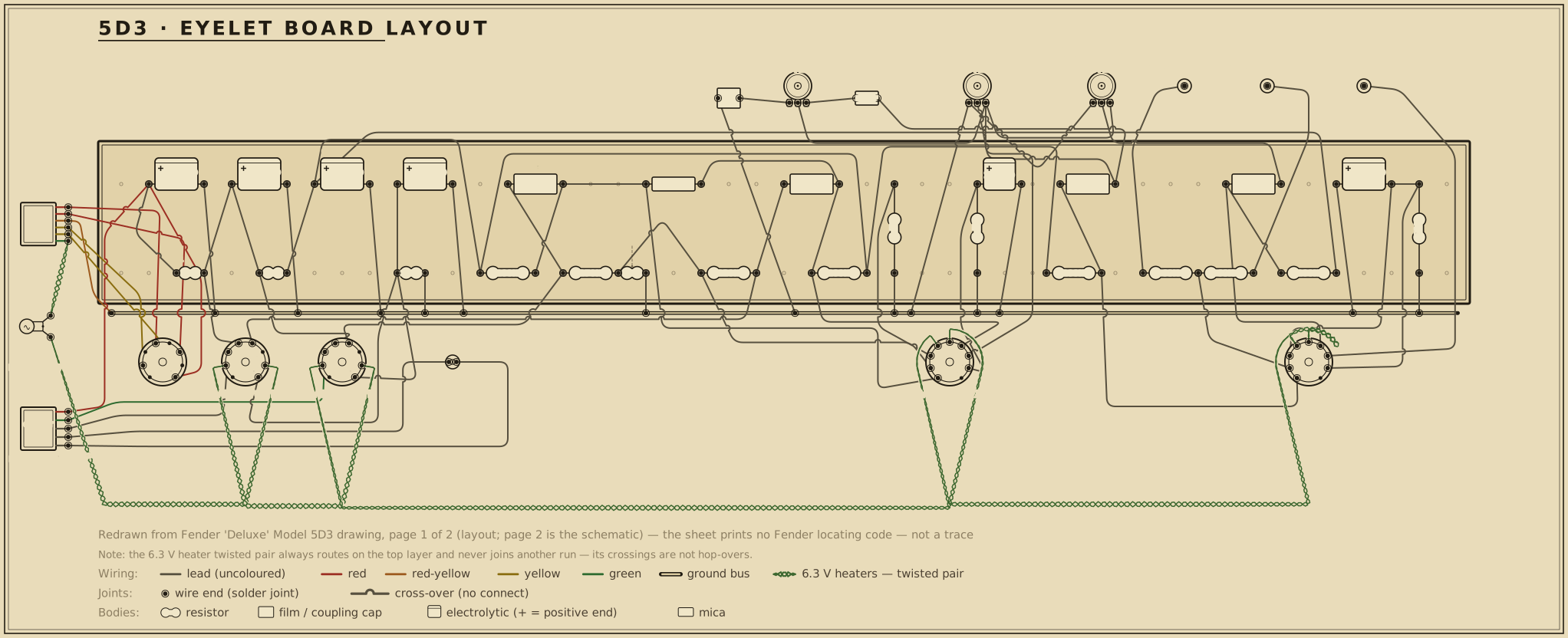
Board layout — redrawn reference diagram · source noted on the drawing Print sheet ↗
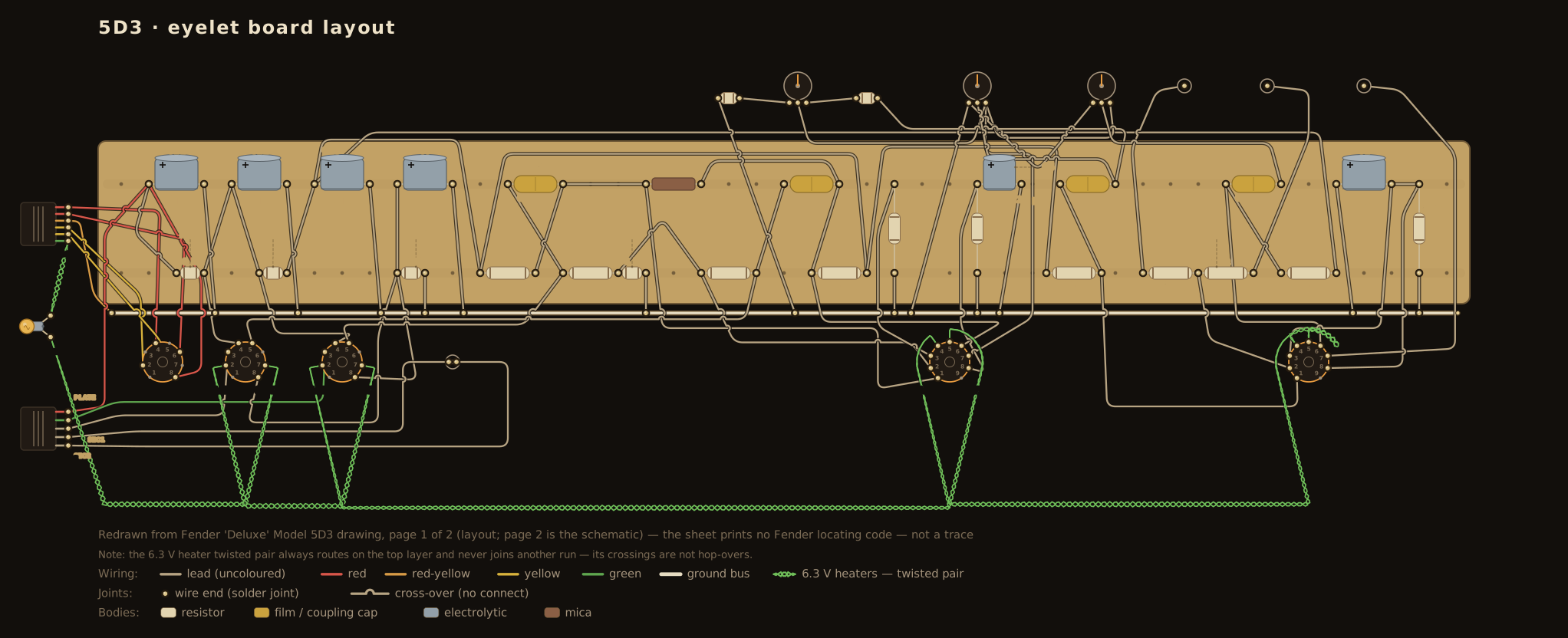
5D3 eyelet board layout — an original diagram redrawn from the published layout drawing, showing the principal parts in the order that drawing places them on the board, drawn in the period layout-sheet style with each value lettered on the part.

Scroll the drawing sideways to read the whole board — the source line and the colour legend run along the bottom of the sheet — or open the full-size diagram in its own tab. Values are lettered on the parts in the period shorthand — .02-400, 250-5, 1MEG: how to read it.

Machine-checked wiring. Every modelled part the operating-point netlist places on this board has been verified in CI, terminal for terminal, to be electrically equivalent to the circuit's simulated netlist. This diagram documents connectivity and part arrangement — it is not a dimensioned 1:1 build template.

Details

The modelled parts are the tube sockets, the plate, cathode and grid-leak resistors, the power-rail droppers, and the coupling and bypass capacitors whose two leads are both named DC nodes; the check proves the same net structure, with no missing or extra connections. Parts outside that DC model — the volume / tone / mixer control-network internals, the negative-bias front end, and the heater chain, pilot lamp and power-transformer / rectifier AC side — are drawn from the cited sources but are not machine-checked; the CI report enumerates every one of their terminals so the boundary is explicit rather than silent.

Board and part positions are drawn at diagram scale, and lead dress, grounding paths, and physical spacing all matter in a high-voltage chassis. If you build from it, verify every connection against the schematic above and the operating-point table below as you go.

Operating point vs. published chart

Chart values read from the published drawing — or, where the drawing carries no voltage chart, from the cited published measurements (never reproduced). The simulated column is this circuit's own netlist solved in ngspice by the run that gates it; every deviation beside it is those two numbers compared, not a separately stated figure. Tolerances are this project's verification targets: tube-pin nodes carry the tolerance the cited source states, or ±20% — the era's printed convention — where it states none, and power rails are held to tighter internal targets.

Node Chart Simulated Deviation Tolerance Note
K66 18 V 16.8 V 6.9% ±20% shared 6V6GT cathode across 250 Ω 5 W — the one node the sibling 5C3 chart transfers to, the output stage being identical
BP2 268.8 V informational — screen node after the first 10 kΩ dropper; the 5C3 chart prints +308 V here, but its lighter preamp draw makes that a loose comparison, not a target
BP3 230.4 V informational — preamp node after the second 10 kΩ dropper; the 5C3 chart prints +280 V here, feeding two 6SC7s through 250 kΩ loads instead of this circuit's four 100 kΩ loads
PAY1 120.2 V informational — 12AY7 plate, channel 1
PAY2 120.2 V informational — 12AY7 plate, channel 2
KAY 1.8 V informational — shared 12AY7 cathode, 820 Ω
P2A 149.0 V informational — 12AX7 driver plate
K2A 1.2 V informational — driver cathode, 1.5 kΩ bypassed
P2B 149.0 V informational — paraphase inverter plate
K2B 1.2 V informational — inverter cathode, 1.5 kΩ unbypassed
GPI 0.0 V informational — paraphase junction (220 kΩ/270 kΩ meeting the 56 kΩ return); idles at 0 V with no grid-current model

Tube-pin nodes are checked at the tolerance the cited source states, or at the era's ±20% convention where it states none; power-rail nodes are held to tighter internal verification targets. Simulated figures are the netlist's DC solution, not measurements from a chassis.

The output stage behind these numbers can be drawn: the load line explorer plots this circuit's 6V6GT pair at the DC operating point its netlist carries — 360 V on the plates with a 250 Ω cathode resistor — and marks where the load line crosses. This circuit is published as a draft, so that operating point is not verified against a published chart: the table and notes above say what each figure rests on.

Parts list

Every designator in this list appears on the schematic above, and every designator on the schematic appears here — the two are checked against each other in both directions, a valve's two halves counting as one bottle (V1A and V1B are both V1). One part the drawing carries as an annotation rather than a numbered symbol is listed here without a designator, and stands outside that check. The 5D3 has three input jacks: one on channel 1 and two on channel 2. The drawing marks no resistor wattages except the 250 Ω 5 W cathode resistor, and prints no transformer impedances or part numbers. The output transformer is numbered T2 under the archive's convention — T1 the power transformer, T2 the output transformer — and no T1 appears because the sheet gives the power transformer neither a part number nor a designator, so it is listed without one.

RefPartValue / ratingRole
RG1 Carbon comp resistor 1 MΩ · ½ W Channel-1 input grid leak (no stopper on this jack)
R2S Carbon comp resistor 68 kΩ · ½ W Channel-2 grid stopper, upper jack
RG2 Carbon comp resistor 1 MΩ · ½ W Channel-2 input grid leak, upper jack
R3S Carbon comp resistor 68 kΩ · ½ W Channel-2 grid stopper, lower jack
RG3 Carbon comp resistor 1 MΩ · ½ W Channel-2 input grid leak, lower jack
RL1 Carbon comp resistor 100 kΩ · ½ W V1A plate load
RL2 Carbon comp resistor 100 kΩ · ½ W V1B plate load
RK1 Carbon comp resistor 820 Ω · ½ W Shared 12AY7 cathode bias
C1 Electrolytic capacitor 25 µF · 25 V Shared 12AY7 cathode bypass
C2 Coupling capacitor 0.05 µF · 600 V V1A → channel-1 volume
C3 Coupling capacitor 0.05 µF · 600 V V1B → channel-2 volume
VR1 Potentiometer 1 MΩ Channel-1 volume
VR2 Potentiometer 1 MΩ Channel-2 volume
VR3 Potentiometer 1 MΩ Tone
C5 Mica capacitor 500 pF Tone — treble path
C6 Film capacitor 0.005 µF · 600 V Tone — cut path to ground
RL3 Carbon comp resistor 100 kΩ · ½ W V2A driver plate load
RK2 Carbon comp resistor 1.5 kΩ · ½ W V2A cathode bias
C4 Electrolytic capacitor 25 µF · 25 V V2A cathode bypass
RL4 Carbon comp resistor 100 kΩ · ½ W V2B inverter plate load
RK3 Carbon comp resistor 1.5 kΩ · ½ W V2B cathode bias (unbypassed)
C14 Mica capacitor 100 pF Across the two inverter plates
RPA Carbon comp resistor 220 kΩ · ½ W V3 grid leak, returned to the paraphase junction
RPB Carbon comp resistor 270 kΩ · ½ W V4 grid leak, returned to the paraphase junction
RPT Carbon comp resistor 56 kΩ · ½ W Paraphase junction → ground
C7 Coupling capacitor 0.05 µF · 600 V V2A plate → V3 grid
C8 Coupling capacitor 0.05 µF · 600 V V2B plate → V4 grid
RK66 Wirewound resistor 250 Ω · 5 W Shared 6V6 cathode bias
C9 Electrolytic capacitor 25 µF · 25 V Shared 6V6 cathode bypass
RD1 Power resistor 10 kΩ Rail dropper B+1 → B+2
RD2 Power resistor 10 kΩ Rail dropper B+2 → B+3
C11 Electrolytic capacitor 16 µF · 450 V Filter, B+1
C12 Electrolytic capacitor 16 µF · 450 V Filter, B+2
C13 Electrolytic capacitor 16 µF · 450 V Filter, B+3
V1 Preamp tube 12AY7 Both input stages (V1A/V1B)
V2 Preamp tube 12AX7 Driver + paraphase inverter (V2A/V2B)
V3 Power tube 6V6GT Push-pull output (upper)
V4 Power tube 6V6GT Push-pull output (lower)
V5 Rectifier tube 5Y3GT Full-wave rectifier (V5A/V5B)
T2 Output transformer push-pull : 8 Ω Push-pull output, with a second 8 Ω jack for an extra speaker; the drawing marks no impedances
Power transformer centre-tapped HT · 6.3 V · 5 V (voltages not marked) HT + heaters + rectifier filament

Circuit story

The last wide-panel Deluxe, and the circuit the famous 5E3 grew out of. It is the revision that retired the octal 6SC7 preamp for the modern nine-pin pair — a 12AY7 feeding a 12AX7 — and it drives its cathode-biased 6V6GT pair through a self-balancing paraphase inverter rather than the cathodyne that would follow. It also drops the negative-feedback loop the 5C3 had introduced, which is why the wide-panel run ends on the open, compressing voice the narrow-panel amps kept. Produced 1954–1955.

Circuit walkthrough (short form)

Three input jacks — channel 1 a single jack on a bare 1 MΩ leak, channel 2 two jacks each through a 68 kΩ stopper onto its own 1 MΩ leak → V1 12AY7 (100 kΩ plate loads, shared 820 Ω cathode bypassed by 25 µF) → 0.05 µF couplers → two 1 MΩ volume pots and the 1 MΩ tone control (500 pF and 0.005 µF) → V2A 12AX7 (100 kΩ plate, 1.5 kΩ bypassed cathode) → V2B paraphase inverter (100 kΩ plate, 1.5 kΩ unbypassed cathode, 100 pF across the two plates) → 0.05 µF couplers → V3/V4 6V6GT pair (no grid stoppers, shared 250 Ω 5 W cathode bypassed by 25 µF) → output transformer with a second jack for an extra 8 Ω speaker. No feedback loop anywhere.

Power: centre-tapped HT → 5Y3GT → three 16 µF/450 V nodes separated by two 10 kΩ droppers: B+1 (output plates and the transformer centre tap) → B+2 (screens) → B+3 (all four preamp plate loads).

How the paraphase balances itself

The inverter is the circuit's signature, and it works nothing like the cathodyne that replaced it. V2A is an ordinary gain stage; its plate drives the upper 6V6's grid through a coupler. That grid is held down by a 220 kΩ leak — but the leak does not go to ground. It meets the lower 6V6's 270 kΩ leak at a junction, and only from there does 56 kΩ run to ground. That junction is also V2B's grid.

So V2B is fed a tap of whatever signal is standing on the two output grids. When the two sides are unequal, the difference appears at the junction, V2B amplifies and inverts it, and its plate pushes the lower grid until the imbalance closes — a see-saw that trims itself. The asymmetric 220 kΩ/270 kΩ pair is the trim: the inverting side is deliberately fed a slightly smaller share so its extra stage of gain does not overshoot. The 100 pF bridging the two plates tames the top end of the loop.

At idle none of this moves a meter. No grid current flows, so the junction, both output grids, and both driver grids all sit at zero, and each 12AX7 section self-biases on its own 1.5 kΩ. The unbypassed cathode on V2B is the one visible asymmetry, and it is deliberate: it holds the inverter's gain down to roughly what the driver in front of it produces.

What changed on the way to the 5E3

The 5D3 and the 5E3 share a tube complement, a tone control, an output stage and a rectifier, but almost every detail between them moved:

5D3 5E3
Phase inverter Self-balancing paraphase (both 12AX7 sections) Cathodyne (one section)
Input jacks 3 4
Couplers 0.05 µF 0.1 µF
Rail droppers 10 kΩ, 10 kΩ 5 kΩ, 22 kΩ
6V6 grid leaks 220 kΩ / 270 kΩ into a 56 kΩ return 220 kΩ each, straight to ground
6V6 grid stoppers none 1.5 kΩ each

The cathodyne swap is the one that matters. It trades the paraphase's self-trimming balance for an inverter balanced by construction — one section's plate and cathode giving the two opposite phases — and it gives up drive to get there. Both circuits spend both halves of the 12AX7: here V2A drives and V2B inverts and amplifies, feeding the lower output grid with gain of its own, while the 5E3 runs V2A as a plain gain stage into a cathodyne that contributes no voltage gain at all. What moves between the two circuits is what each half does, not how many stages there are. The rest of the table is smaller change: larger couplers, a different dropper split, and grid stoppers this circuit does without.

Verification

The published 5D3 sheets supply every component value but print no voltage chart — only Fender's ±20 % measurement notice. The 5C3 drawing immediately before it does print one, and the two circuits share the power transformer class, the 5Y3GT, all three 16 µF filter nodes, both 10 kΩ droppers and the whole output stage, so its reservoir figure of 360 V is the value B+1 is driven at here and its +18 V across the 6V6 cathode resistor is a fair target. Simulation puts that cathode at 16.8 V — 6.9 % off, comfortably inside the era's convention.

The rails are reported, not compared. The 5C3 prints +308 V and +280 V for the screen and preamp nodes, but it feeds a pair of 6SC7s through 250 kΩ plate loads where this circuit feeds four 100 kΩ loads, so more current crosses the same two 10 kΩ droppers and the rails must land lower: simulation gives 269 V and 230 V, with the 12AY7 plates at 120 V and both 12AX7 plates at 149 V. Those are consistent, but they are this circuit's numbers checked against a different preamp's chart, which is not a verification. The 5D3 stays a draft until a voltage chart measured on a 5D3 is available.

Sources