5F8-A High‑power Tweed Twin‑style · 1958–1960 · 80 W

draft
Schematic — redrawn in KiCad · scroll to zoom, drag to pan
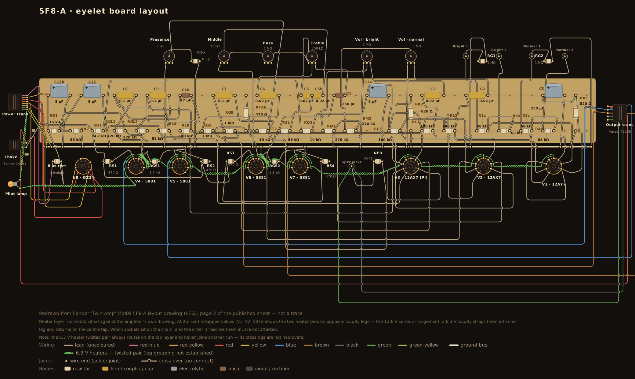
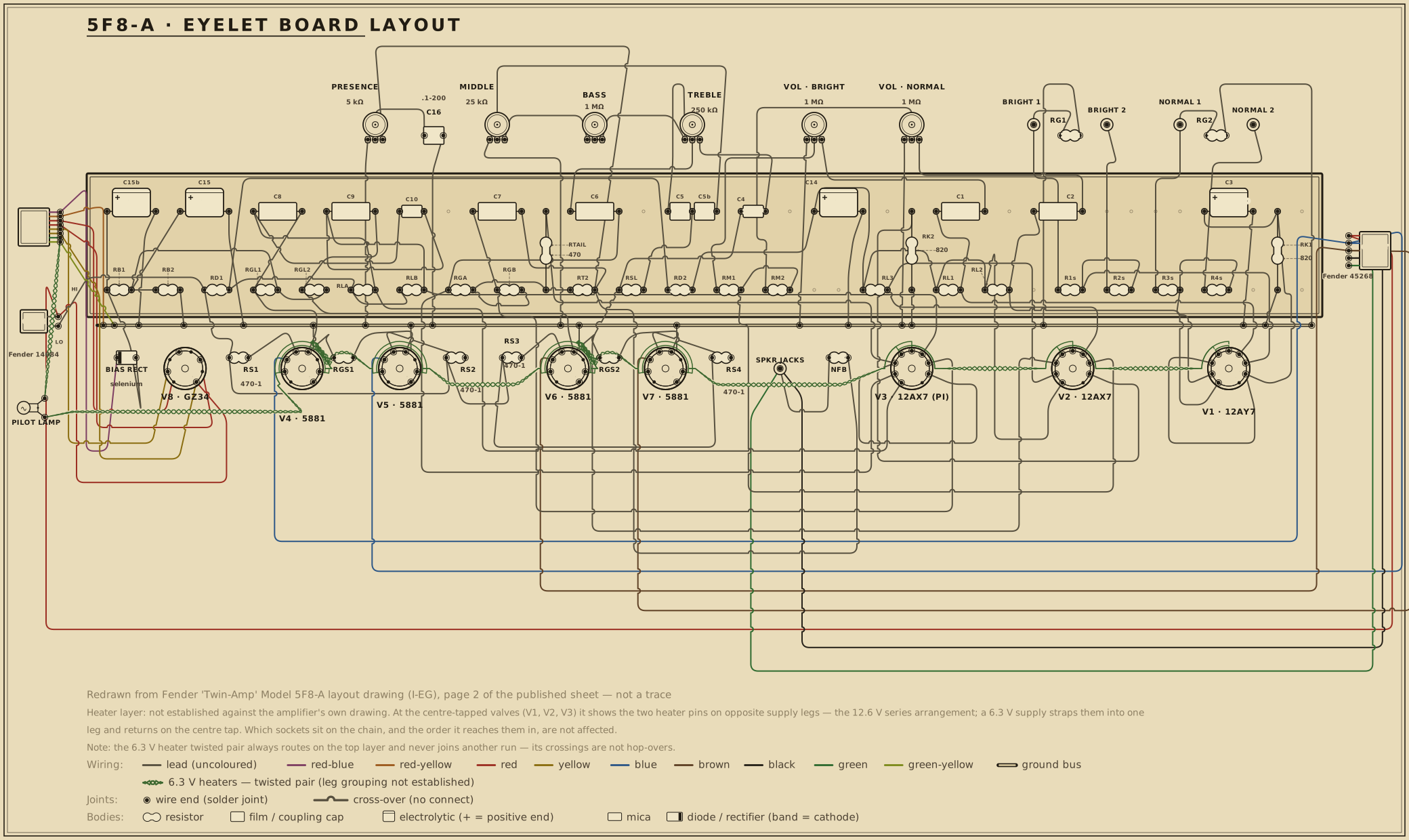
Board layout — redrawn reference diagram · source noted on the drawing Print sheet ↗
5F8-A eyelet board layout — an original diagram redrawn from the published layout drawing, showing the principal parts in the order that drawing places them on the board, drawn in the period layout-sheet style with each value lettered on the part.

Scroll the drawing sideways to read the whole board — the source line and the colour legend run along the bottom of the sheet — or open the full-size diagram in its own tab. Values are lettered on the parts in the period shorthand — .02-400, 250-5, 1MEG: how to read it.

This diagram documents connectivity and part arrangement — it is not a dimensioned 1:1 build template.

Details

Board and part positions are drawn at diagram scale, and lead dress, grounding paths, and physical spacing all matter in a high-voltage chassis. If you build from it, verify every connection against the schematic above and the operating-point table below as you go.

Operating point vs. published chart

Chart values read from the published drawing — or, where the drawing carries no voltage chart, from the cited published measurements (never reproduced). The simulated column is this circuit's own netlist solved in ngspice by the run that gates it; every deviation beside it is those two numbers compared, not a separately stated figure. Tolerances are this project's verification targets: tube-pin nodes carry the tolerance the cited source states, or ±20% — the era's printed convention — where it states none, and power rails are held to tighter internal targets.

Node Chart Simulated Deviation Tolerance Note
BP2 395 V 395.0 V 0.0% ±8% screens node after the choke (DCR estimated at 130 Ω)
BP3 355 V 354.7 V 0.1% ±8% PI supply node after the 4.7 kΩ
BP4 295 V 296.2 V 0.4% ±8% preamp node after the 10 kΩ dropper
PAY1 145 V 152.0 V 4.8% ±20% 12AY7 plate, bright channel
PAY2 145 V 152.0 V 4.8% ±20% 12AY7 plate, normal channel
KAY 2.2 V 2.4 V 7.5% ±20% shared 12AY7 cathode, 820 Ω
P2A 165 V 166.7 V 1.0% ±20% V2A plate = cathode-follower grid (direct-coupled)
K2A 1 V 1.1 V 6.2% ±20% V2A cathode, 820 Ω unbypassed
KCF 165 V 167.0 V 1.2% ±20% cathode-follower output; the sheet prints +165 on both sides of the direct coupling, so the follower runs at about −1 V grid-to-cathode
PPIA 230 V 236.0 V 2.6% ±20% PI plate, 82 kΩ 5% side
PPIB 225 V 226.4 V 0.6% ±20% PI plate, 100 kΩ 5% side
KPI
chart disputed
28.5 V 41.1 V 44.3% not gated
The printed tail figures fit a tail the drawing does not show.

The printed plates (+230 V through 82 kΩ and +225 V through 100 kΩ, both off +355 V) carry 1.52 + 1.30 = 2.82 mA, and 2.82 mA through a 10 kΩ returned straight to ground is 28.2 V at the junction and 29.6 V at these cathodes — the printed +27 V and +28.5 V. But the I-EG schematic and layout both land that 10 kΩ on a node of its own, returned to ground through the 56 kΩ feedback resistor and the 5 kΩ presence pot's track in parallel (4.6 kΩ); at the same 2.82 mA that puts the junction at 41.2 V and these cathodes at 42.5 V. Simulation follows the drawn tail.

JPI
chart disputed
27 V 39.8 V 47.5% not gated
The other half of the same contradiction — see KPI.

The printed plates' 2.82 mA through the 10 kΩ alone gives 28.2 V, which fits the printed +27 V only if the 10 kΩ returns to ground; through the drawn foot (56 kΩ ∥ 5 kΩ = 4.6 kΩ) the same current puts the junction at 41.2 V.

PRES 12.5 V informational — the tail's foot, where the 10 kΩ, the 56 kΩ feedback resistor, the presence pot's track and the V3B grid's 0.1 µF meet; the drawing prints no figure here
GA1 −41 V −41.0 V 0.0% ±8% fixed bias via the 220 kΩ leaks from the −41 V supply
SA1 394.2 V informational — 5881 screen after its 470 Ω; the sheet prints no screen figure

Tube-pin nodes are checked at the tolerance the cited source states, or at the era's ±20% convention where it states none; power-rail nodes are held to tighter internal verification targets. A node marked chart disputed is excluded from that check — its printed value contradicts the rest of the chart, and the note says how; its deviation is shown for the record, not as a result. Simulated figures are the netlist's DC solution, not measurements from a chassis.

The output stage behind these numbers can be drawn: the load line explorer plots this circuit's 5881 quartet at the DC operating point its netlist carries — 397 V on the plates with a −41 V grid bias — and marks where the load line crosses. This circuit is published as a draft, so that operating point is not verified against a published chart: the table and notes above say what each figure rests on.

Parts list

Every designator in this list appears on the schematic above, and every designator on the schematic appears here — the two are checked against each other in both directions, a valve's two halves counting as one bottle (V1A and V1B are both V1). Two parts the drawing carries as annotations rather than numbered symbols are listed here without designators, and stand outside that check. The sheet's own note reads: all resistors are ½ W 10% unless otherwise marked, so a wattage appears below only where the drawing letters one (470 Ω 1 W screens; 1 W on both rail droppers) and a tolerance only where it letters one (5% on the two phase-inverter plate loads). The drawing shows two jacks on each channel and this schematic draws both, with all four 68 kΩ stoppers. The presence pot and its 0.1 µF wiper cap are chassis wiring, and the negative-feedback resistor mounts on the eyelet board beside the tail's 10 kΩ, as the factory layout places it; all three carry designators (RNF, VR6, C16) and are drawn. The 100 pF bright cap mounts on the bright volume pot's own lugs, inside the tone/volume network the DC model abstracts, so it is listed without a designator and annotated on the schematic rather than drawn.

RefPartValue / ratingRole
R1s Carbon comp resistor 68 kΩ Bright channel, jack 1 grid stopper
R2s Carbon comp resistor 68 kΩ Bright channel, jack 2 grid stopper
R3s Carbon comp resistor 68 kΩ Normal channel, jack 1 grid stopper
R4s Carbon comp resistor 68 kΩ Normal channel, jack 2 grid stopper
RG1 Carbon comp resistor 1 MΩ Bright input grid leak, at the jacks
RG2 Carbon comp resistor 1 MΩ Normal input grid leak, at the jacks
RL1 Carbon comp resistor 100 kΩ V1A plate load
RL2 Carbon comp resistor 100 kΩ V1B plate load
RK1 Carbon comp resistor 820 Ω Shared 12AY7 cathode bias
C3 Electrolytic capacitor 250 µF · 6 V Shared 12AY7 cathode bypass
C1 Coupling capacitor 0.02 µF · 400 V V1A → bright volume
C2 Coupling capacitor 0.02 µF · 400 V V1B → normal volume
VR1 Audio-taper potentiometer 1 MΩ Bright volume (100 pF bright cap across it)
VR2 Audio-taper potentiometer 1 MΩ Normal volume
RM1 Carbon comp resistor 270 kΩ Bright-channel mixer
RM2 Carbon comp resistor 270 kΩ Normal-channel mixer
RL3 Carbon comp resistor 100 kΩ V2A plate load
RK2 Carbon comp resistor 820 Ω V2A cathode bias, unbypassed
RKCF Carbon comp resistor 100 kΩ Cathode-follower load
RSL Carbon comp resistor 56 kΩ Tone-stack slope resistor
C4 Mica capacitor 250 pF Tone stack — treble
VR3 Linear potentiometer 250 kΩ Treble (the factory layout page marks it 250K LIN.)
C5 Film capacitor 0.02 µF · 400 V Tone stack — bass (node B → the treble-lug/bass node)
C5b Film capacitor 0.02 µF · 400 V Tone stack — middle (node B → the middle pot's wiper)
VR4 Audio-taper potentiometer 1 MΩ Bass (1M AUD. on the layout page); wired as a rheostat down the ladder
VR5 Linear potentiometer 25 kΩ Middle (the second 0.02 µF lands on its wiper; its full track stands in the ground leg)
C6 Coupling capacitor 0.02 µF · 400 V Tone stack → phase-inverter grid
RGA Carbon comp resistor 1 MΩ PI grid leak (V3A), returned to the tail junction
RGB Carbon comp resistor 1 MΩ PI grid leak (V3B), returned to the tail junction
RLA Carbon comp resistor 82 kΩ · 5% PI plate load (V3A)
RLB Carbon comp resistor 100 kΩ · 5% PI plate load (V3B)
RTAIL Carbon comp resistor 470 Ω PI tail bias
RT2 Carbon comp resistor 10 kΩ PI tail (junction → foot)
C10 Mica capacitor 47 pF Across the two PI plates
C7 Film capacitor 0.1 µF · 200 V V3B grid AC-ground to the tail foot
RNF Carbon comp resistor 56 kΩ Negative feedback, speaker → the phase-inverter tail foot
VR6 Linear potentiometer 5 kΩ Presence — its track from the tail foot to ground, 0.1 µF on the wiper
C16 Film capacitor 0.1 µF · 200 V Presence wiper to ground
C8 Coupling capacitor 0.1 µF · 400 V PI (V3A) → the V4/V5 output pair
C9 Coupling capacitor 0.1 µF · 400 V PI (V3B) → the V6/V7 output pair
RGL1 Carbon comp resistor 220 kΩ Grid leak for the V4/V5 pair, from the −41 V bias line
RGL2 Carbon comp resistor 220 kΩ Grid leak for the V6/V7 pair, from the −41 V bias line
RGS1 Carbon comp resistor 1.5 kΩ Grid stopper between the V4 and V5 grids
RGS2 Carbon comp resistor 1.5 kΩ Grid stopper between the V6 and V7 grids
RS1 Carbon comp resistor 470 Ω · 1 W V4 screen resistor
RS2 Carbon comp resistor 470 Ω · 1 W V5 screen resistor
RS3 Carbon comp resistor 470 Ω · 1 W V6 screen resistor
RS4 Carbon comp resistor 470 Ω · 1 W V7 screen resistor
RD1 Power resistor 4.7 kΩ · 1 W Rail dropper B+2 → B+3
RD2 Power resistor 10 kΩ · 1 W Rail dropper B+3 → B+4
L1 Filter choke Fender 14684 B+1 → B+2 (screens)
C11 Electrolytic capacitor 20 µF · 600 V Filter, B+1
C11b Electrolytic capacitor 20 µF · 600 V Filter, B+1 (the sheet draws two cans on this node)
C12 Electrolytic capacitor 20 µF · 600 V Filter, B+2
C13 Electrolytic capacitor 20 µF · 600 V Filter, B+3
C14 Electrolytic capacitor 8 µF · 450 V Filter, B+4
D1 Rectifier (bias) selenium (silicon diode in modern builds) Bias supply rectifier
RB1 Carbon comp resistor 15 kΩ Bias supply series resistor
RB2 Carbon comp resistor 56 kΩ Bias supply bleeder
C15 Electrolytic capacitor 8 µF · 150 V Bias supply filter, −41 V line
C15b Electrolytic capacitor 8 µF · 150 V Bias supply reservoir, rectifier side of the 15 kΩ
V1 Preamp tube 12AY7 Both input stages (V1A/V1B)
V2 Preamp tube 12AX7 Second stage + cathode follower (V2A/V2B)
V3 Preamp tube 12AX7 Long-tailed-pair phase inverter (V3A/V3B)
V4 Power tube 5881 Output, 82 kΩ side of the inverter (paralleled with V5)
V5 Power tube 5881 Output, 82 kΩ side of the inverter (paralleled with V4)
V6 Power tube 5881 Output, 100 kΩ side of the inverter (paralleled with V7)
V7 Power tube 5881 Output, 100 kΩ side of the inverter (paralleled with V6)
V8 Rectifier tube GZ34 Full-wave rectifier (V8A/V8B)
T3 Output transformer Fender 45268 Push-pull-parallel output into two speakers; the drawing prints no secondary impedance
Power transformer Fender 7993 · 300-0-300 V HT + heaters + rectifier filament
Mica capacitor 100 pF Bright cap across VR1, mounted on the pot (annotation only on schematic)

Circuit story

The last tweed Twin, and the circuit that sets the shape of every Twin after it: the 5F6-A's front end and long-tailed-pair inverter driving four 5881s in two parallel pairs instead of two, on a supply stiff enough to hold them. Two channels of two jacks feed a 12AY7; a 12AX7 stage direct-coupled to a cathode follower drives the treble/middle/bass stack; a second 12AX7 splits the phase; and the output quartet runs fixed-bias at −41 V with 470 Ω 1 W screen resistors and a 1.5 kΩ stopper bridging each pair's grids. A GZ34 rectifies, a choke follows the reservoir, and a standby switch stands ahead of both.

Circuit walkthrough (short form)

Bright and normal channels, two jacks each (68 kΩ stoppers, 1 MΩ leaks) → V1 12AY7 (100 kΩ plates, shared 820 Ω cathode with 250 µF bypass) → 0.02 µF couplers → 1 MΩ volume pots (100 pF bright cap) → 270 kΩ mixers → V2A 12AX7 (100 kΩ plate, 820 Ω cathode, unbypassed) → V2B cathode follower, DC-coupled (100 kΩ cathode load) → TMB tone stack (56 kΩ slope, 250 pF treble, two 0.02 µF; 250 kΩ/1 MΩ/25 kΩ pots) → 0.02 µF → long-tailed-pair PI: 82 kΩ and 100 kΩ 5% plates, 470 Ω + 10 kΩ tail, both 1 MΩ grid leaks returned to the tail junction, 47 pF across the plates, 0.1 µF holding the second grid at the tail foot → two 0.1 µF couplers → four 5881s in two parallel pairs, fixed-biased at −41 V, into the 45268 output transformer and two speakers, with 56 kΩ of negative feedback returning to the tail foot alongside the 5 kΩ presence pot and its 0.1 µF wiper cap.

Power: 300-0-300 (PT 7993) → GZ34 → standby → +397 V plates (two 20 µF cans) → choke (14684) → +395 V screens → 4.7 kΩ 1 W → +355 V phase inverter (20 µF) → 10 kΩ 1 W → +295 V preamp (8 µF). Bias supply: selenium rectifier, 15 kΩ/56 kΩ, two 8 µF/150 V cans → −41 V.

The output stage, as the drawings wire it

The four bottles are two parallel pairs, not two push-pull pairs, and the distinction is the whole circuit:

  • Each phase of the inverter drives one pair through one 0.1 µF coupler and one 220 kΩ grid leak. The leak hangs on the coupler node, which is the first bottle's grid.
  • The 1.5 kΩ stopper stands between the pair's two grids, not in series with the coupler. On the factory board it is a single resistor bridging one socket's grid pin to the next socket's — which is exactly what the schematic draws, and what a builder wiring from the layout sheet will find.
  • Both bottles of a pair share a plate connection to one end of the output transformer's primary, and both cathodes go straight to ground. Only the screens are individual: each has its own 470 Ω 1 W resistor to the +395 V node, and all four are socket-mounted rather than on the eyelet board.

The tone network, as the drawings wire it

The published 5F8-A schematic and its factory layout sheet draw the same ladder the 5F6 and 5F6-A print — not the textbook redrawing of these parts — and the schematic and layout here follow the sheets:

  • The 250 pF treble capacitor and the 56 kΩ slope resistor both leave the cathode-follower output.
  • One 0.02 µF capacitor runs from the slope resistor's foot to the node shared by the treble pot's lower lug and the bass pot.
  • The bass pot is a rheostat in series down the ladder, its wiper strapped into the treble-lug node.
  • The other 0.02 µF runs from the slope foot to the middle pot's wiper, so the Middle control slides the capacitor's injection point along a 25 kΩ leg that never leaves the circuit.
  • The stack's output is the treble pot's wiper alone, and the middle pot's foot runs straight to ground; the presence control sits at the phase-inverter tail instead.

What this page does not claim

  • The secondary impedance. The drawing prints the output transformer's part number (45268) and nothing about its windings, so no impedance is stated here and the amp carries no iron rating. Two speakers, no figure.
  • The power rating and the production years. The sheet prints neither. The 80 W figure and the 1958–1960 span come from a separate published source, cited below, rather than from the drawing.
  • The bias supply's own voltages. Only the −41 V line it delivers is printed, so the simulation drives that node as an ideal source rather than modelling the selenium rectifier and its 15 kΩ/56 kΩ divider.
  • The 100 pF bright cap. It mounts on the bright volume pot's own lugs, inside the volume network the DC model abstracts, so it is annotated on the schematic rather than drawn as a two-terminal part.

Where the model simplifies, and why

The DC deck drives +397 V at the reservoir and derives everything below it. One simplification is worth stating plainly, because it is visible on the sheet:

  • The choke is modelled as 130 Ω of winding resistance, an estimate. The sheet prints 397 V on one side of it and 395 V on the other — the same 2 V the 5F6-A's sheet prints across the same part number, 14684.

The tail foot, and a chart that does not fit it

The drawing runs the 10 kΩ tail's foot to the presence pot's hot lug and grounds the pot's cold lug, with the 56 kΩ feedback resistor and the second grid's 0.1 µF landing on the same foot: the schematic draws the four on one vertical, and the layout on one eyelet. The model carries that foot as drawn. The 56 kΩ (back to the speaker, DC ground through the output transformer) and the pot's 5 kΩ track are both DC returns, and simulation puts the foot at +12.5 V.

The printed chart does not fit it. Its plate figures (355 → 230 V through 82 kΩ, 355 → 225 V through 100 kΩ) imply 2.82 mA of tail current, and 2.82 mA through the 10 kΩ alone is 28.2 V — the printed +27 V junction, with +28.5 V at the cathodes. Through the drawn foot the same current would put the junction at 41.2 V. The two tail figures are therefore shown as disputed: the page prints them beside the simulated +39.8 V junction and +41.1 V cathodes rather than bending the circuit to match.

Verification — against the printed factory chart

The I-EG drawing prints a full voltage chart, and simulation matches twelve of its fourteen compared nodes (the 5881 screen carries no chart value and is informational only): rails within 0.4 %, every gated tube pin within 7.5 %, against the sheet's own stated convention of ±20 % read with an electronic voltmeter. The other two are the tail figures above, disputed.

Reading the chart off a scan

The I-EG sheet circulates in copies of very different quality, and its chart is lettered small. Every voltage on this page was read from a 693 ppi capture (6368 × 3218 for the schematic page); the widely mirrored copy carries the same sheet at 1506 × 841, roughly 100 ppi, and its chart digits do not resolve. Two figures come out wrong if you read them from the coarse copy anyway:

node coarse copy 693 ppi
supply either side of the choke +377 / +375 +397 / +395
phase-inverter cathode +22.5 V +28.5 V

The cathode is the one to check against your own copy, because the circuit settles it without the drawing: it has to sit above the tail junction's +27 V, since its current reaches that junction through the 470 Ω. A figure below +27 V cannot be right, whatever the scan appears to say.

Component values and topology read cleanly off either copy. It is only the chart that needs the resolution.
Sources

Found a value, a date or a claim on this page that doesn't match its source? Report a correction for 5F8-A ↗ — the form opens with this page and its circuit id filled in, and asks what you checked it against. Every correction is reviewed before anything changes.