Verification details
What these checks meanEach check covers a different part of this reference. The circuit badge records the DC comparison and maintainer review.
View checks, findings and exclusions
- DC operating point Verified
- 7 reference nodes are within tolerance. Maintainer verification is recorded for 2026-07-18; changes since then are awaiting maintainer re-review.
- The circuit's facts (netlist, reference voltages, parts list, both drawings' connections, capacitor polarity marks and heater declarations) have changed since the maintainer's review, or no review fingerprint is on record yet. The badge stands on its date until the maintainer re-reviews.
- This compares simulated DC conditions with the cited reference. It does not test sound, physical construction or every part of the circuit.
- Schematic against DC model Checked
- Connectivity of modelled components is checked on every change.
- Parts outside the DC model need separate checks and source review.
- Board against DC model Checked
- Connectivity of modelled components is checked on every change.
- This does not establish heater wiring or physical spacing.
- Schematic against board No open findings
- No disagreement is listed in the published comparison.
- A finding identifies a difference or a coverage gap. The factory source must decide which drawing, if either, needs correction.
- 0 sheet-only parts are explicitly excluded. Heaters and the pilot lamp are checked separately.
- Heater and filament wiring Checked
- The declared heater circuits cover the drawing and pass their separate wiring check.
- Capacitor polarity Checked
- 4 capacitor markings agree with the model's voltage ordering.
- This check uses DC voltage ordering; source review establishes markings the model cannot decide.
Archive revision ebddc3f. Published corrections. These checks do not certify a physical build.
Machine-checked drawing. This sheet is checked in CI against the netlist the simulation solves: every component the netlist models is proved to have its terminals on the same nodes in this drawing as in that netlist, so the picture and the maths cannot drift apart.
Details
The check compares connectivity, and only as far as the netlist reaches. It does not check component values, and it does not prove the netlist itself a faithful reading of the factory drawing — that rests on the operating-point comparison below and on the cited sources. The netlist is a DC model, so what it leaves out is drawn here but outside this check: the supply front end ahead of the first rail, transformer winding resistance, the volume / tone / mixer control networks and the capacitors inside them, and the heater and AC-side wiring. Separate checks cover drawing-to-board agreement, declared heater circuits and polarity where the model can decide it; see Verification details for their coverage and findings. Every abstraction this circuit relies on is declared as reviewable data in its own sch_map.yaml, and the CI report enumerates each terminal left unchecked.
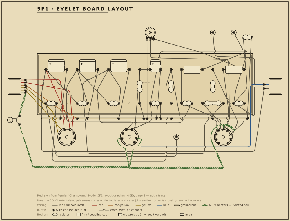
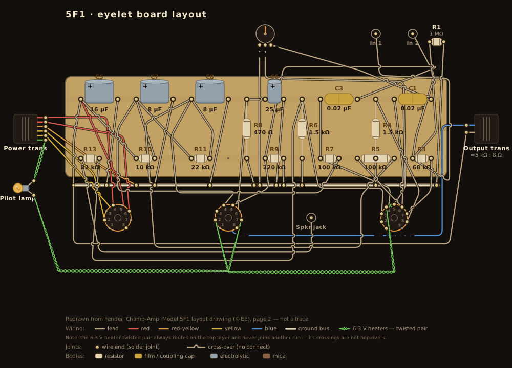
Scroll the drawing sideways to read the whole board — the source line and the colour legend run along the bottom of the sheet — or open the full-size diagram in its own tab. The whole board is on screen, source line and colour legend included. Open the full-size diagram in its own tab to zoom in or print it. Values are lettered on the parts in the period shorthand — .02-400, 250-5, 1MEG: how to read it.
Machine-checked wiring. Every modelled part the operating-point netlist places on this board has been verified in CI, terminal for terminal, to be electrically equivalent to the simulated netlist this circuit is verified against. This diagram documents connectivity and part arrangement — it is not a dimensioned 1:1 build template.
Details
The modelled parts are the tube sockets, the plate, cathode and grid-leak resistors, the power-rail droppers, and the coupling and bypass capacitors whose two leads are both named DC nodes; the check proves the same net structure, with no missing or extra connections. Parts outside that DC model — the volume / tone / mixer control-network internals, the negative-bias front end, and the heater chain, pilot lamp and power-transformer / rectifier AC side — are drawn from the cited sources but are outside this DC equivalence check. Separate checks compare the drawings and examine declared heater circuits and polarity; see Verification details for their coverage and findings.
Board and part positions are drawn at diagram scale, and lead dress, grounding paths, and physical spacing all matter in a high-voltage chassis. If you build from it, verify every connection against the schematic above and the operating-point table below as you go.