GA40 Gibson GA‑40 Les Paul‑style · 1956–1962 · 15 W

draft
Schematic — redrawn in KiCad · scroll to zoom, drag to pan
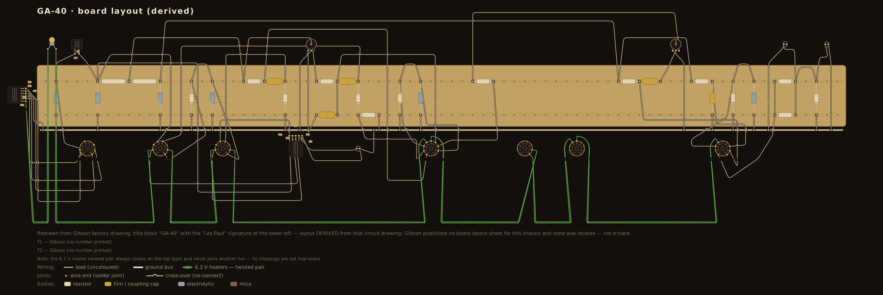
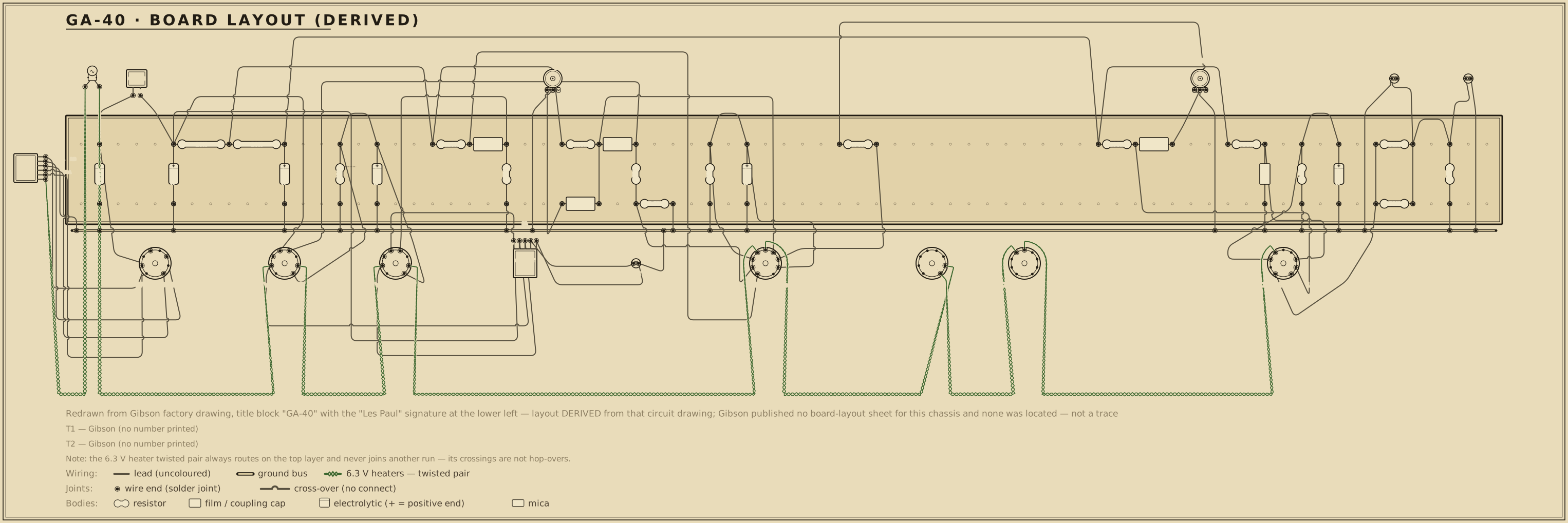
Board layout — redrawn reference diagram · source noted on the drawing Print sheet ↗
GA40 board layout — an original diagram reconstructed from the redrawn schematic (no factory layout sheet exists), showing the principal parts in board order, drawn in the period layout-sheet style with each value lettered on the part.

Scroll the drawing sideways to read the whole board — the source line and the colour legend run along the bottom of the sheet — or open the full-size diagram in its own tab. Values are lettered on the parts in the period shorthand — .02-400, 250-5, 1MEG: how to read it.

Machine-checked wiring. Every modelled part the operating-point netlist places on this board has been verified in CI, terminal for terminal, to be electrically equivalent to the circuit's simulated netlist. This diagram documents connectivity and part arrangement — it is not a dimensioned 1:1 build template.

Details

The modelled parts are the tube sockets, the plate, cathode and grid-leak resistors, the power-rail droppers, and the coupling and bypass capacitors whose two leads are both named DC nodes; the check proves the same net structure, with no missing or extra connections. Parts outside that DC model — the volume / tone / mixer control-network internals, the negative-bias front end, and the heater chain, pilot lamp and power-transformer / rectifier AC side — are drawn from the cited sources but are not machine-checked; the CI report enumerates every one of their terminals so the boundary is explicit rather than silent.

Board and part positions are drawn at diagram scale, and lead dress, grounding paths, and physical spacing all matter in a high-voltage chassis. If you build from it, verify every connection against the schematic above and the operating-point table below as you go.

Operating point vs. published chart

Chart values read from the published drawing — or, where the drawing carries no voltage chart, from the cited published measurements (never reproduced). The simulated column is this circuit's own netlist solved in ngspice by the run that gates it; every deviation beside it is those two numbers compared, not a separately stated figure. Tolerances are this project's verification targets: tube-pin nodes carry the tolerance the cited source states, or ±20% — the era's printed convention — where it states none, and power rails are held to tighter internal targets.

Node Chart Simulated Deviation Tolerance Note
P1 175 V 133.7 V 23.6% ±20% channel-1 5879 anode, 100 kΩ load off the +265 rail. Reads low: see the honest residual above — the 5879 model's screen-current law is anchored at Vg2=100 V and this stage runs at +95 V on a 750 kΩ dropper
SG1 95 V 130.1 V 37.0% ±20% channel-1 5879 screen grid, fed through 750 kΩ and bypassed to ground by 0.05 µF — the node that sets a pentode's current, and the node the model misses
K1 4 V 4.9 V 23.2% ±20% channel-1 5879 cathode, 3.3 kΩ bypassed by 20 µF. The chart's own plate and screen currents over that resistor give +3.7 V, so the printed +4 V and the drawing's 3.3 kΩ agree; the simulated figure inherits the screen error above
P4A 135 V 139.5 V 3.3% ±20% phase-inverter anode, driver half — 220 kΩ load off the +280 rail. The chart prints one figure for both halves in its E(p1)/E(p2) columns
P4B 135 V 139.5 V 3.3% ±20% phase-inverter anode, inverted half — 220 kΩ load, the half whose grid hangs on the 470 kΩ/7.5 kΩ paraphase divider
K4 1.25 V 1.3 V 2.2% ±20% phase-inverter shared cathode over ONE 1 kΩ resistor (20 µF bypass) — both halves on it, which is why 1.25 V and not half that
KOUT 18.5 V 18.3 V 1.0% ±20% shared 6V6GT cathode over the single 200 Ω resistor (20 µF bypass) — the amp's entire bias arrangement, for both bottles, with no bias supply anywhere
NPARA 0.0 V informational — the paraphase tap itself, where the 470 kΩ from the first output grid meets the 7.5 kΩ to ground and drives the inverter's second grid. Idles at exactly 0 V: there is no grid-current model in the archive's first-generation tube fits
G5 0.0 V informational — first 6V6GT control grid, behind the 0.02 µF coupler; its DC return is the paraphase divider itself rather than a leak of its own
G6 0.0 V informational — second 6V6GT control grid, behind its own 0.02 µF coupler with a 470 kΩ leak to ground
NIN1 0.0 V informational — the channel-1 jack node, where the 1 MΩ leak meets both 51 kΩ input resistors. No grid current flows, so this node sets no operating point

Tube-pin nodes are checked at the tolerance the cited source states, or at the era's ±20% convention where it states none; power-rail nodes are held to tighter internal verification targets. Simulated figures are the netlist's DC solution, not measurements from a chassis.

The output stage behind these numbers can be drawn: the load line explorer plots this circuit's 6V6GT pair at the DC operating point its netlist carries — 310 V on the plates with a 200 Ω cathode resistor — and marks where the load line crosses. This circuit is published as a draft, so that operating point is not verified against a published chart: the table and notes above say what each figure rests on.

Parts list

Every designator in this list appears on the schematic above, and every designator on the schematic appears here — the two are checked against each other in both directions, a valve's two halves counting as one bottle (V1A and V1B are both V1). Eight parts the drawing carries as annotations rather than numbered symbols are listed here without designators, and stand outside that check. Capacitor values are open at DC and do not enter the operating-point netlist; they are listed for completeness, and the ones whose BOTH leads land on a named DC node are modelled anyway so the push-pull phase and the bypass placement are fixed in the data. The drawing prints no wattages and no tolerances anywhere, so the era's implied ½ W is stated for the small resistors and the shared output cathode resistor — a part passing 92 mA at 18.5 V, some 1.7 W — carries no rating this entry can cite. A published restoration of a GA-40 records the supply-can complement as 20/10/10/10 µF at 450 WVDC; three of those four are lettered below, and the fourth is most likely on the +280 inverter rail, where this reading places no can. The gap is left visible rather than filled.

RefPartValue / ratingRole
V1 Tube 5879 Channel 1 preamp pentode
V2 Tube 5879 Channel 2 preamp pentode — the tremolo-modulated channel (stage not lettered here; see the header)
V3 Tube 6SQ7 Tremolo phase-shift oscillator (excluded from the netlist; network not lettered here)
V4 Tube 12AX7 Paraphase phase inverter, both triodes
V5 Tube 6V6GT Output beam power tube
V6 Tube 6V6GT Output beam power tube
V7 Rectifier tube 5Y3GT Full-wave rectifier
T1 Power transformer Gibson (no number printed) Mains transformer — centre-tapped HT winding, 5 V rectifier winding, 6.3 V heater winding. The drawing prints the windings and no part number
T2 Output transformer Gibson (no number printed) Output transformer, centre-tapped primary; the centre tap is the post-choke supply node the screens also sit on
L1 Choke 3 H Smoothing choke between the reservoir and the screen/output-transformer node
Jack socket 1/4 in Channel 1 input, first jack (annotation only)
Jack socket 1/4 in Channel 1 input, second jack (annotation only)
RIN1 Carbon comp resistor 51 kΩ · ½ W Channel 1 first-jack series resistor into the grid
RIN2 Carbon comp resistor 51 kΩ · ½ W Channel 1 second-jack series resistor into the same grid
RG1 Carbon comp resistor 1 MΩ · ½ W Channel 1 grid leak — at the jack end, ahead of both 51 kΩ resistors
RL1 Carbon comp resistor 100 kΩ · ½ W Channel 1 plate load, off the +265 preamp rail
RS1 Carbon comp resistor 750 kΩ · ½ W Channel 1 screen dropper, +265 rail → screen grid — the resistor the factory chart's own arithmetic confirms to 749 kΩ
CS1 Film capacitor 0.05 µF Channel 1 screen bypass to ground
RK1 Carbon comp resistor 3.3 kΩ · ½ W Channel 1 cathode bias
CK1 Electrolytic capacitor 20 µF Channel 1 cathode bypass (no voltage rating printed)
CV1 Coupling capacitor 0.01 µF Channel 1 plate → volume coupler
VR1 Potentiometer 1 MΩ Channel 1 volume — the drawing prints no taper. It is wired the unusual way round: the coupler drives the WIPER and the mixing resistor leaves the top of the track, with the bottom end grounded. Channel 2's volume is wired identically
RM1 Carbon comp resistor 470 kΩ · ½ W Channel 1 mixing resistor, volume control → inverter grid. It leaves the TOP of the volume track, not the wiper: the drawing brings the 0.01 µF coupler onto the wiper instead (see VR1)
RL4A Carbon comp resistor 220 kΩ · ½ W Inverter driver plate load, off the +280 rail
RL4B Carbon comp resistor 220 kΩ · ½ W Inverter inverted-side plate load, off the same rail
RK4 Carbon comp resistor 1 kΩ · ½ W Inverter cathode bias — ONE resistor shared by both triodes
CK4 Electrolytic capacitor 20 µF Inverter cathode bypass (no voltage rating printed)
RPA Carbon comp resistor 470 kΩ · ½ W Paraphase divider, upper leg — first output grid down to the inverted half's grid; doubles as that output grid's leak
RPB Carbon comp resistor 7.5 kΩ · ½ W Paraphase divider, lower leg — the inverted half's grid down to ground. 7.5/477.5 is 1/63.7, which is what a 12AX7 on a 220 kΩ load gives back
CT1 Film capacitor 0.005 µF Tone capacitor, inverter driver anode → Tone control
VR3 Potentiometer 1 MΩ Tone — the amplifier's only tone control, working treble to bass, wired with its wiper to ground and sitting between the phase inverter and the output tubes
CC1 Coupling capacitor 0.02 µF Inverter driver anode → V5 grid
CC2 Coupling capacitor 0.02 µF Inverter inverted-side anode → V6 grid
RGL6 Carbon comp resistor 470 kΩ · ½ W V6 grid leak — the only one of the two that goes to ground
RKO Power resistor 200 Ω SHARED 6V6GT cathode bias resistor — the whole bias arrangement for the pair, with no bias supply anywhere in the amp. The drawing prints no wattage
CKO Electrolytic capacitor 20 µF 6V6GT cathode bypass (no voltage rating printed)
CF1 Electrolytic capacitor 20 µF Reservoir can, ahead of the choke — the 5Y3GT cathode node the chart reads +315 V
CF2 Electrolytic capacitor 10 µF Post-choke smoothing — the +310 V node that is also the output-transformer centre tap and both 6V6GT screens
RD1 Carbon comp resistor 10 kΩ · ½ W +310 node → +280 inverter rail
RD2 Carbon comp resistor 10 kΩ · ½ W +280 inverter rail → +265 preamp rail
CF3 Electrolytic capacitor 10 µF +265 preamp rail smoothing
Speaker 12 in Single 12-inch speaker (annotation only). Published accounts of this revision name a Jensen P12Q; the drawing letters no make
Film capacitor 0.02 µF Mains-side capacitor to ground, selected onto one line leg or the other by the polarity switch (annotation only)
Toggle switch SPST Mains on/off, marked SW on the drawing, in one line leg (annotation only)
Fuse 3 A Mains fuse, in the other line leg (annotation only)
Toggle switch SPDT Polarity switch — the era's line-reverse arrangement, which chooses which mains leg the 0.02 µF capacitor grounds; drawn beside the 115–125 V 50–60 cycle mains legend (annotation only)
Pilot lamp 6.3 V Pilot lamp, marked P.L. across the 6.3 V heater winding (annotation only)

Circuit story

Gibson's answer to the tweed combo, and almost nothing about it is a Fender idea. Where Fullerton put a twin triode at the front of an amplifier, Gibson put a pentode: one 5879 per channel, a nine-pin bottle whose data sheet is titled for audio-amplifier applications critical as to microphonics, leakage noise, and hum — a valve chosen for living six inches from a twelve-inch speaker. Where Fender's tone stack sits between two gain stages, the GA-40 has no stack at all: a single capacitor and a single control hang off the phase inverter's own anode, and that one knob is the whole tone circuit. And where a blackface amplifier splits phase with a long-tailed pair, this one uses a paraphase — a second triode fed a divided copy of the first one's output — which was already old-fashioned when this sheet was drawn and stayed in Gibson amplifiers long after.

The model number is not a wattage. A GA-40 makes about 15 W from a cathode-biased pair of 6V6GTs.

Which revision this is

The GA-40 ran from 1952 to late 1962, and the model number covers at least three different amplifiers. The 1954 drawing is a genuinely different machine: three octal 6SJ7s, a 6SN7 phase inverter, three 6V6GTs — two on the output and one doing the tremolo — and a 5V4G rectifier. This entry documents the later, 5879 circuit: two 5879 pentodes, a 6SQ7 tremolo oscillator, a 12AX7 paraphase inverter, two 6V6GTs and a 5Y3GT. Published accounts put that front end from 1956 and count no fewer than five Les Paul GA-40 variants across the model's life, so the 5879 circuit itself covers more than one drawing.

This sheet is undated and carries no revision box, so this entry cannot say which of those it is. The era bracket runs from the earliest year the cited sources put the 5879 front end to the last year the model was catalogued: an outer bound over the 5879 revisions, and labelled as one.

The paraphase, and the arithmetic in it

The inverter is the part of this amplifier worth reading twice. Both 12AX7 halves have 220 kΩ anode loads and share one 1 kΩ cathode resistor with a 20 µF bypass. The driver half takes the mixed channel signal, and its anode drives the first 6V6GT's grid through 0.02 µF. The 470 kΩ that leaks that grid does not go to ground: it goes to the other triode's grid, where 7.5 kΩ carries on to ground. That divider is the whole trick.

7.5 / (470 + 7.5) is 1 / 63.7. A 12AX7 working into a 220 kΩ load has very nearly that gain, so the inverted half receives 1/64 of the first grid's swing and returns it full size and upside down. The second 6V6GT's 470 kΩ leak does go to ground, because its grid is not a divider tap. Two 470 kΩ resistors, doing two different jobs, is what a paraphase looks like on a drawing.

The factory chart confirms the reading three ways over. Both anodes print +135 V off a +280 V rail, which puts 0.66 mA through each 220 kΩ load; the two currents together over one 1 kΩ resistor give 1.32 V against a printed +1.25 V. The simulation lands +139 V and +1.28 V — inside 4 %.

The output stage

Two 6V6GTs, cathode-biased on one shared 200 Ω resistor with a 20 µF bypass and no bias supply anywhere in the amplifier. The screens are not dropped at all: they sit straight on the post-choke supply node, the same node as the output-transformer centre tap, which is why the chart prints +310 V for both. The anodes read +305 V — the 5 V is the half-primary's own resistance, which this corpus's netlists do not carry.

18.5 V over 200 Ω is 92.5 mA of cathode current for the pair, 46 mA each — and a few of those milliamps are screen current, so the anodes take roughly 42 mA at 305 V. That is about 13 W of plate dissipation against a 12 W design-centre rating: over the sheet, and exactly where every cathode-biased pair of the period sat. The simulation reads 18.3 V at the cathode and 42.0 mA at the anode.

Channel 1, and what the chart proves about the reading

Channel 1's 5879 has a 100 kΩ anode load and a 750 kΩ screen dropper, both off the +265 V preamp rail, with the screen bypassed to ground by 0.05 µF and the cathode on 3.3 kΩ with 20 µF across it. Every one of those values can be checked against the chart that was measured through them:

lettered resistor with the printed voltage gives
100 kΩ anode load anode +175 V from a +265 V rail 0.90 mA of anode current
750 kΩ screen dropper screen +95 V from the same rail 0.227 mA of screen current
3.3 kΩ cathode resistor both currents through it +3.72 V, against a printed +4.0 V

Two of the printed voltages and three resistors read off a low-resolution scan predict the third printed voltage to 7 %. The values are right.

One detail of that channel is worth drawing carefully, because it is easy to redraw wrong: the volume control is wired the unusual way round. The 0.01 µF coupler does not land on the top of the 1 MΩ track — it lands on the wiper, and the 470 kΩ mixing resistor leaves the top of the track, with the bottom end grounded. Channel 2's own 1 MΩ volume is wired identically ahead of its 100 kΩ mixing resistor, so it is the arrangement rather than a slip of the pen. It still works as a volume control — the track below the wiper shunts the signal and the track above it passes what is left — and at DC it makes no difference at all, which is why the operating point is unmoved either way. The schematic and the board layout draw it as the sheet draws it.

The simulation is the part that misses, and the operating-point table on this page records it node by node. The corpus's 5879 model is a single-anchor fit at Va = 250 V, Vg2 = 100 V, and in this model form the screen-current law has no plate-voltage term at all. Run at the screen voltage this circuit uses it draws roughly a third of the screen current the real valve does, so the 750 kΩ dropper leaves the screen at +130 V instead of +95 V and the extra screen volts pull the anode down to +134 V. Anode −24 %, screen +37 %, cathode +23 %, all outside the era's ±20 %.

Some of that gap is not the model's. The chart states its own convention — voltages to chassis with 20,000 O.P.V. meter — and 20,000 ohms per volt on a 250 V range is 5 MΩ. Five megohms across a node fed through 750 kΩ draws 19 µA, worth about 14 V of extra drop in that dropper, so the screen this chart printed is meaningfully lower than the screen the amplifier ran. It is the most meter-sensitive node on the sheet, and it is the node the simulation misses by the most. The same loading is worth only about 3 V at the anode, behind 100 kΩ, and nothing at all at the cathode.

What remains is a limitation of the archive's first-generation tube fits — a single-anchor model asked to work far from its anchor. It is one of the three reasons this circuit is a draft, and it is left visible rather than hidden behind an ungated node.

Channel 2 and the tremolo — read, not lettered

Both are on the drawing and neither is in the netlist or the parts list. This is the honest edge of what the surviving scan supports, so here is what is legible and what is not.

Channel 2 takes the same input arrangement as channel 1 — two jacks, a 51 kΩ series resistor each, one 1 MΩ leak — onto a second 5879 with a 2.2 kΩ cathode resistor. Its anode load reads 510 kΩ, and its output runs through a ladder of five 0.005 µF series capacitors with 1 MΩ shunts between them before reaching its own 1 MΩ volume control and a 100 kΩ mixing resistor into the inverter grid. That ladder is a progressive bass cut, and a published bench feature on a 1956 example describes this channel's front end as carrying a filter network of the Vox AC10/AC15 kind, which is what it is.

The tremolo is a 6SQ7 phase-shift oscillator with 510 kΩ resistors in its anode chain, a 500 kΩ Frequency control and 0.01 µF / 0.05 µF ladder capacitors, feeding a 100 kΩ resistor into a 500 kΩ Depth control. It does not gate the signal path. It modulates channel 2's screen and supply — swinging the gain of a pentode by moving the electrode that sets a pentode's gain. Seth Lover designed it.

What is not legible is the resistor that feeds channel 2's screen, and how the Depth network loads it. The factory chart makes the consequence unmissable: channel 2's screen prints +32 V where channel 1's prints +95 V, off the same +265 V rail. Nothing about channel 2's operating point can be derived without that resistor, and this entry will not invent it.

The chart's channel-2 row does not close on any reading of the drawing this scan supports, and that is worth stating plainly rather than quietly. Take the row as printed — anode +130 V, screen +32 V, cathode +1.45 V. The cathode figure over a 2.2 kΩ resistor is 0.66 mA of total current, but the anode figure off a +265 V rail through the 510 kΩ load is only 0.27 mA, which would leave 0.4 mA flowing in a screen sitting 30 V above ground — far more screen current than plate current, which a sharp-cutoff pentode does not do. Note also that the row shares two of its three figures exactly with the 6SQ7 row directly beneath it (+130 and +1.45), the kind of coincidence a transcription slip produces. Both possibilities — an unresolved screen network, or an error on the chart — stay open here, and neither is resolved by guessing.

Any future re-reading of this circuit should start with a better scan of the channel-2 and tremolo half of the sheet, or with a second published drawing of the same revision. Until then, the parts list letters what can be built and says so.

Supply

5Y3GT into a 20 µF reservoir (+315 V at its cathode on the chart), a 3 H choke, then 10 µF at the +310 V node that feeds both screens and the output-transformer centre tap. From there 10 kΩ to the +280 V inverter rail and another 10 kΩ to the +265 V preamp rail with its own 10 µF can. A published restoration records the can complement as 20/10/10/10 µF; this reading places three of the four, and the fourth most likely sits on the +280 V rail. That gap is recorded in the parts list rather than filled in.

Because the droppers between those three rails also carry channel 2 and the tremolo — neither of them modelled — the netlist drives all three rails at the chart's own printed figures instead of deriving a chain that is missing half its load. That is the same convention the 6G6-B entry uses, and the reason none of the three appears as a gated node: a driven node proves nothing.

Mains

A polarity switch — the era's line-reverse arrangement — chooses which side of the 115–125 V line the 0.02 µF capacitor grounds. The on/off switch sits in one leg and a 3 A fuse in the other. A 6.3 V pilot lamp hangs on the heater winding. Do not build the mains side as drawn; it predates grounded three-wire practice.
Sources